Test systems often use a small quantity of instruments to address a large number of signals. This design approach constrains cost but also limits measurement throughput. Conversely, a system with sufficient instruments to test all the signals as quickly as possible provides the highest throughput but generally is unaffordable.
The classical example of a low-cost test system switches one digital voltmeter (DVM) among several signals. If only two signals are involved, the switch can be described in the usual shorthand nomenclature as a single-pole double-throw (SPDT) capable of connecting the DVM�the single pole�to either of the two signals. If both the high and low sides of the signal must be switched, a double-pole double-throw (DPDT) configuration would be suitable. For four signals, a DP4T switch could be used.
Applications also exist for multiple poles beyond two. For example, a 4PDT switch could support four-wire or Kelvin-connected, Ohms measurement on two components. A 6PDT switch would provide driven guarding as well as four-wire Ohms. No doubt, this type of nomenclature can be extended indefinitely.
Multiplexers are described in a similar poles and throws sense, expressed as n � m where n is the number of poles and m is the number of throws. However, manufacturers do not agree on the order of the n and m. Some vendors term a single pole eight-way multiplexer a 1�8, and others call it an 8�1. In a multiplexer, all the poles generally are switched together. For example, a 2�8 multiplexer could be used to switch one of eight differential signals to a differential voltmeter.
The same n � m notation is used to describe a switch matrix, but in a true matrix, any one of the n rows can be connected to any one of the m columns. For example, a 2�8 matrix can simultaneously connect either or both of its rows to any number of the columns. If desired, this matrix could mimic a differential multiplexer but because of the greater number of switches involved would have worse performance and higher cost.
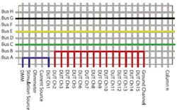
Usually, a matrix is used to switch multiple instruments among many input channels. Chris Cahoon, a design engineer at B&B Technologies, discussed a column-oriented example shown in Figure 1.
�Instruments, sources, and DUTs are assigned to columns. A voltage source is applied to ch1 of a device under test, and a DMM measures the voltage,� he said. �Simultaneously, the unused inputs are all grounded. In this arrangement, the matrix rows act like buses to connect together groups of columns. You can imagine a test sequence in which each of the DUT channels is tested in turn with the other channels grounded.
�Alternatively, in a row-based arrangement, you would have the test instruments and sources on different rows,� Mr. Cahoon continued. �The columns are dedicated to the DUTs. Any combination of rows and columns can be selected, so it�s important that the switch is correctly programmed to prevent, for example, two sources being shorted together.�
In some cases, the increased cost of a true matrix can be avoided by using a blocking matrix that allows only one row to be connected to a particular column. Depending on the switching flexibility you may require, a few multiplexers can be combined to create a so-called sparse matrix, supporting only a subset of all possible row-column combinations.
Also, the order in which rows and columns are switched may be important. Generally, break-before-make switches are used to ensure that even momentary shorts do not occur between incompatible signals. When developing the test program, switch configuration software can monitor the programmed instructions and inhibit the switch change if damage could occur from such a connection. Use of a matrix makes safety of the test system and the DUT the responsibility of the test programmer.
An RF Test Example
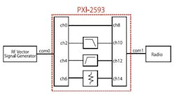
The simplified test system shown in Figure 2 is based on the setup used by Bloomy Controls to perform an intermediate frequency (IF) rejection ratio measurement on an FM radio with a 10.7-MHz IF. Both the FM signal power and carrier frequency are controlled. The radio�s audio output is measured across a 4-? load to simulate a speaker. Measurement instruments, not shown, are connected directly to the radio inputs and outputs.
Both the RF signal and the radio are tuned to 90.1 MHz. In the first part of the test, the -3-dB limiting sensitivity measurement, the RF power is reduced from a reference level until the audio output drops by 3 dB. This RF power level is used later to calculate the radio�s IF rejection.
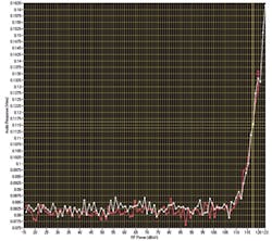
Next, the signal�s carrier frequency is reduced to 10.7 MHz but the radio remains tuned to 90.1 MHz. The audio output level is monitored as the RF signal power level is increased. Figure 3a shows the response to two different signal generators. The audio output rapidly increases for signal power above 72 or 90 dB�V depending on the generator.
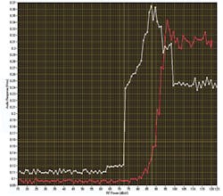
In Figure 3b, the audio response does not increase significantly until the input power reaches between 110 and 115 dB�V. The improvement in the uniformity of response to the two different generators as well as a larger IF rejection value result from the low-pass filter connected between ch2 and ch10 in the PXI-2593 Multiplexer. Because the signal generator output noise level became greater as the 10.7-MHz IF amplitude was increased, a low-pass filter that reduced noise above 10.7 MHz significantly improved measurement accuracy.
The Multiplexer
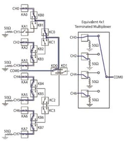
The National Instruments PXI-2593 Switch Module can be used unterminated configured as a quad 3�1, a dual 8�1 or a single 16 or 17�1 multiplexer. Adding external 50-? terminations supports operation as a dual 4�1 or single 8�1 terminated multiplexer for high-frequency signals exceeding 500 MHz. A detailed schematic diagram of this configuration is shown in Figure 4.
Typically, complete switch modules are specified by their isolation, return loss, and insertion loss. In practice, use of a vector network analyzer to characterize performance of modules or individual relays very quickly provides complete S-parameter information. The isolation and loss quantities can be derived from S-parameters.
Certain simplifications often are assumed, such as symmetry. For example, if a relay is physically the same viewed from the input or output, then the transmission from output to input (S12) and from input to output (S21) will be equal or very nearly the same.
In the radio test setup, the 500-MHz switch specification greatly exceeded the 90.1-MHz maximum signal frequency. However, switch specifications in addition to bandwidth are critical for RF applications. For example, how well is the switch matched to the test system�s 50-? characteristic impedance? A poor match, equivalent to a large voltage standing wave ratio (VSWR), would cause reflections resulting in a standing wave pattern and a distorted test signal.
From the PXI-2593 datasheet, the VSWR from DC to 200 MHz is guaranteed to be <1.4:1. A plot of typical performance shows it just above 1.1:1. VSWR is defined as VSWR = (1+|?|)/(1-|?|) where |?| is the magnitude of the reflection coefficient. For these VSWR limits, the corresponding range of the input reflection coefficient is 0.167 to 0.048 or about 17% to 5%.
The return loss often is quoted rather than the reflection coefficient. The two quantities are related by return loss = -20 log (|?|); for the radio test example, it is 15.5 dB to 26.4 dB. A larger number means that the ratio between the power passed by the switch and that reflected is greater. In other words, a larger return loss value means that more of the input power appears at the output.
Considering the same VSWR range but viewed with respect to the output power gives rise to the insertion loss parameter. If 16.7% of the signal power was lost because it was reflected at the input, 83.3% arrived at the output. The ratio of 0.833:1 is the basis of the insertion loss calculation. Insertion loss = 10 log (output/input) = 0.8 dB to 0.2 dB corresponding to VSWRs of 1.4:1 and 1.1:1, respectively. A graph of typical performance shows about 0.2 dB at 100 MHz.
Isolation
When a switch is open and the signal path is intended to be completely cut off, a small portion of that signal still will couple to the output. Isolation describes the fraction of the input signal power that couples to the output. A switch�s isolation always degrades with increasing frequency because of the capacitance across the open contacts. However, different types of relays can provide sufficiently low capacitance to support switching 1-GHz or 2-GHz signals and even signals up to 40 GHz.
For example, the highest density switch modules use small reed relays as the switching elements. Reed relays, in addition to being small, are very reliable, low cost, and available with a wide range of specifications. Nevertheless, because the two reeds are close to each other within a glass tube, the minimum capacitance of an open switch is about 0.2 pF.
The BGA-mounted Coto Technology B40 Reed Relay is an example of a practically leadless device designed to match a 50-? transmission line. According to the Coto website, �In the BGA relays, the signal path between the BGA signal input and output is designed as an RF transmission line, with an RF impedance close to 50 ? throughout the relay. This is achieved using a well-matched combination of coplanar waveguide and coaxial structures with very little impedance discontinuity through the relays.�1
This relay has an impressive 11.5-GHz, -3-dB bandwidth, but its isolation at 5 GHz is only 10 dB. Although the relay is well matched, resulting in a good return loss of about 35 dB at 1 GHz and 20 dB at 5 GHz, 10% of the input signal leaks to the output at 5 GHz when the relay is open.
The isolation of the PXI-2593 Multiplexer is not specified but typically is greater than 90 dB at 100 MHz. How can this large isolation figure be achieved if reed relays are used in the switch? The answer is that reed relays aren�t used. A note in the spec identifies the type of relay as, �electromechanical, latching.� A relay configuration that allows the contact size, positioning, and separation to be optimized overcomes the restrictions of a reed construction.
As an example of an electromechanical relay, the Omron Electronic Components G6Y High-Frequency Relay provides at least 65 dB isolation at 900 MHz. This performance implies about 0.002-pF stray capacitance. This amount of capacitance corresponds to 84-dB isolation at 100 MHz, and curves of typical performance show >90 dB at 100 MHz. The conclusion is that electromechanical relays, although larger than reed relays, can have much better characteristics when open.
Of course, the G6Y is not just any electromechanical relay with an armature and actuating coil. That generic description also applies to 10-A power relays or the old multipole telephone relays. No, the G6Y is intended to be used with microstrip lines on a double-sided PCB. Grounding is very important, and the data sheet confirms that improved performance can be obtained with more vias connecting the component- and solder-side ground planes. Typical insertion loss and return loss are 0.2 dB and 25 dB at 1 GHz, respectively. The relay is not specified above 2.5 GHz.
Although the PXI-2593 Multiplexer does not use reed relays, it is possible to achieve very high isolation using reed relays at high frequency. A Tee configuration of two relays in series with a third relay to ground from the midpoint shunts capacitively coupled signals to ground. This approach requires three relays, and the mismatch of the two relays in series will degrade the overall insertion loss.
To go very much higher in frequency than a few gigahertz and achieve good loss and isolation performance, a coaxial relay is required. Radiall manufactures these very specialized switches that typically provide 70-dB isolation, 0.4-dB insertion loss, and 1.7:1 VSWR at 26.5 GHz.
To achieve this level of performance, coaxial switches integrate a Tee configuration. The input and output pins are physically small and far apart to minimize capacitance. However, when the circuit is open, the moving contact that bridges the pins to close a circuit is grounded, shunting any capacitively coupled signal.
In all types of relays, latching usually implies a permanent magnet in the magnetic path. This means that only a short pulse is required to change the switch state, the permanent magnet holding the contacts in the selected position.
Conclusion
Each type of switching application requires a specialized solution. Just as general-purpose, high-frequency, and microwave switches have different characteristics to meet unique requirements, so too, for example, does very low-level switching.
|
FOR MORE INFORMATION |
| B&B Technologies | Test System Integration | www.rsleads.com/604ee-190 |
| Bloomy Controls | Test System Integration | www.rsleads.com/604ee-191 |
| Coto Technology | Reed Relays | www.rsleads.com/604ee-192 |
| Keithley Instruments | Instrumentation and Switching | www.rsleads.com/604ee-193 |
| National Instruments | PC-Based Switching | www.rsleads.com/604ee-194 |
| Omron Electronic Components | Electromechanical Relays | www.rsleads.com/604ee-195 |
| Radiall | Coaxial Relays | www.rsleads.com/604ee-196 |
A Keithley Instruments application note discusses the increase in signal settling time that may result from suddenly applying a large signal to the cabling in a test system: �The way source voltage or current is applied to a DUT can have a significant effect on how quickly the DUT and test instruments settle. A large, sudden voltage applied to the DUT can result in a longer I-V settling tail due to the capacitance of the cables and DUT and dielectric absorption properties of the probe card. If one measures too quickly, the resulting measurement will be unstable because there is a high probability that the measurement was taken during the exponential rise or fall portion of the I-V response curve. Adding an arbitrarily long delay can result in inefficient and slow measurements.
�Often, it is better to break the large voltage step into smaller steps using the sweep capabilities of the instruments. By approaching the final voltage using smaller voltage steps, it is possible to improve the settling characteristics of the measurement. Another approach is to take advantage of the steady-state measurement commands of [some] parametric testers�.A steady state measurement command will instruct the tester to continue measuring until a user-defined change criterion is met, for example, measure until the reading changes by no more than 3%.�2
Although these comments refer to flat-panel testing and the measurement of very small leakage currents, they serve to illustrate that switching is seldom as straightforward as it may first appear. In light of the problems that could have been caused by a multiplexer with marginal performance at 100 MHz, perhaps Bloomy Controls� choice of the 500-MHz PXI-2593 was prudent rather than extravagant.
References
1. www.cotorelay.com/RF_Parameter_Measurement.pdf
2. Cimino, C. and Rose, D., New Test Realities for Evolving FPD Technologies, Keithley Instruments, 2006, www.keithley.com/applications/flat/#2
Acknowledgement
Thanks to Peter Blume of Bloomy Controls and Chris Cahoon at B&B Technologies for their contributions to this article.
April 2006
About the Author
Comment About the Article
To join the conversation, and become an exclusive member of Electronic Design, create an account today!

Leaders relevant to this article: