Multisite Test Strategy For SIP Mobile Technologies
The challenge of SIPs goes beyond what it takes to assemble them.
Increasing functionality and performance in ICs have driven manufacturers to work with wider and more challenging packaging solutions. As a result, the test strategies need to verify functionality.
Looking back about 10 years ago, 30% to 35% of the IC market demand was driven by consumer products and more than 50% by computing applications. With an increasing shift from Information Technology (IT) infrastructure driven investments to broad consumer products, the priorities and technical requirements are dramatically changing.
Today, more than 60% of the IC market is dominated by the price-sensitive consumer market with a major force being hand-held portable consumer products that demand increased computing power and an increased variety of functionality but at a reduced cost. The costs associated with assembly and especially device test have come under extreme pressure. In turn, the need to integrate more functions in one device with a quick market entry is driving the use of SIPs.
SIPs have emerged as a device pack-aging solution in response to the significant convergence of computing and mobility technologies into one package impacting cost, size, and power consumption. Consider the 1950s when computers were the size of a room. Compare that to what laptop computers or even cell phones can provide today.
As technologies progress, devices are shrinking to meet the requirement of smaller is better. Consumer products also demand flexibility, driving an ever-increasing variety of functionality in devices. More and more manufacturers are requiring integration of dissimilar devices into one package.
Who Uses SIPs?
Consumer products ranging from cell phones, radios, and hand-held GPS to automotive accessories like remote entry are using SIPs. However, the biggest driver has been wireless applications, PDAs, and Bluetooth communications products.
Device manufacturers evaluating a SIP implementation strategy see the biggest benefit in the measured cost savings for the development phase. Using chips already designed, there is a significant savings compared to the time it takes to develop a system-on-a-chip (SOC) from scratch. Enhancing this major benefit is the reduced risk of assembling readily available predesigned, pretested chips in one package vs. creating new silicon.
In the wireless space, the capability to add and remove functions either to change price points or meet special market requirements very quickly is a key part of the SIP benefits. This allows for tuning of the manufacturing strategy to particular market needs.
A classic example of this is meeting varying communications standards: code division multiple access (CDMA) in the United States vs. global system for mobile communications (GSM) for Europe and time division multiple access (TDMA) in Asia. By swapping out SIP elements, manufacturers can leverage a basic design and customize it over multiple market geographies.
Assessing Test Solutions
As manufacturers think about implementing SIPs, they have to take into account not only the manufacturing process, but also the test strategy because, from a test standpoint, SIPs present some real challenges. For example, a SIP device with three different die in the same package requires three test solutions, which could drive the potential need for three different testers. Three different testers with three production interfaces, three test programs, and three separate operating environments requiring test engineers to be trained for each might be viewed as the only available solution. This is not an ideal scenario for the test engineer or the manufacturer.
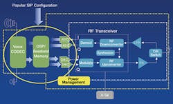
Figure 1 shows a typical block diagram of a cell phone and its various major components. The circled area represents some of the most popular technologies being merged into a SIP. The digital processor, memory, analog components, converters, RF front-end components, and often power management are some of the elements integrated on a SIP.
Focusing on the components in that portion of the cell phone, let�s consider what�s needed for a SIP test strategy. First, it requires memory test and SOC test. Second, when packaged into a SIP, there may be constraints on access to individual die and the number of test points.
Packaged devices may not have enough pins or the internal interconnect scheme may limit access. As a result, the test strategy or the types of tests you perform and how you perform them may have to change to accommodate the limited access. Existing test programs for the individual die may not be directly portable when the die are packaged in the SIP. Challenges also can arise around device initialization and synchronization.
Besides meeting the technical requirements, the solution for providing both memory and SOC test also must be cost-effective to reach the price points demanded by consumer end products. If a test solution requires multiple insertions, there is the potential to damage the device as the number of insertions increases, leading to yield problems.
Multiple insertions also add to the cost of test. For the best test economics, reduced insertion solutions in conjunction with multisite or parallel test strategies supported on one tester are needed to achieve the desired cost of test.
Most importantly, manufacturers are under pressure to make sure that what goes into the package works. They do perform minimal functional testing to ensure the die is good but often do not do performance testing until the die is in the package.
This approach has inherent yield risks because as there may be four die in one package with three working and one bad. This results in discarding all four die, which ultimately creates a yield drop and increases cost.
Memory Impact on SIP Test
Wireless cell phones are adding more and more functions that require lots of available memory. As a result, incorporating memory into the SIP has become common practice.
Typically, memory will come from a third-party memory supplier, arriving as a known-good die and delivered with a test program that validates the die as good. The company packaging the SIP device has to perform a backside grind process on that known-good die to reduce its thickness. SIPs can only be an acceptable packaging alternative if the packaged device does not exceed height restrictions of the end-use product.
One major risk created by the mechanical grinding is impacting the structural integrity of the memory die, which in turn, can impact its electrical characteristics. As a result, the memory die can become less capable of retaining data over the full performance range of the application.
SIP manufacturers have experienced yield loss as much as 0.5% to 3% due to the grinding and assembly process. For that reason, functional testing of the die in the package may be required after the grinding and assembly process. A key factor to a SIP test strategy is implementing the right amount of memory test.
When assessing a test strategy optimized for memory test time, the test engineer needs to consider SOC test, which is on the order of 3 to 5 seconds and perhaps as many as 10 seconds, to do full 100% performance test. Compare that to testing a 256M DRAM where test times can be 2 to 4 minutes for full performance and functional testing. In the case where you need to perform full memory testing in conjunction with testing the other SIP components, the economics and the strategy of parallelism and efficiency appear to drive toward a solution of two testers and two insertions.
Comparing Alternatives
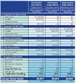
Table 1 displays three strategies for testing a SIP device. The column on the left highlights a dual-insertion strategy with two platforms: two different testers where each device needs to be tested on each tester. In this example, one tester is a memory tester capable of testing 64 devices in parallel, and the second tester is an SOC tester capable of testing four sites in parallel. The basic assumption is that the memory component of the SIP requires full functional testing under various power supply conditions and test parameters.
IEEE European Test Symposium, May 2006
MS = mixed signal
The middle column represents a single platform strategy using two SOC testers. One tester is configured to address the memory test, and one tester is configured to address the SOC test. This requires two test programs and two device interfaces.
This strategy assumes that the SIP contains a memory that is a known-good die and that reduced functional test can be performed to ensure proper functionality. Also assumed is that the price of the memory tester is less than the cost of the tester for the SOC test.
The column on the right represents a fully integrated single-tester, single-insertion test strategy using an SOC tester. The assumptions with this test strategy are that the memory is a known-good die and that the manufacturing process is capable of assembling the SIP without damage to the memory die. Consequently, only a few very simple functional tests are required to ensure proper interconnects and that no damage occurred during the assembly of the SIP.
The final section of Table 1 shows the throughput capability of the different test strategies. Also included is the yield impact that handling the device for multiple insertions can have. An assumption of 3% yield impact was used for purposes of the example in the dual-insertion strategies.
From the throughput perspective, if two minutes are required for full functional memory test under a variety of operating conditions, then if the dual-insertion and dual-platform strategy is used, it produces a total test time per device of 1.875 seconds. If the memory test patterns can be reduced by two-thirds because the SIP contains a known-good die and only requires a basic set of memory test patterns to verify functionality, then a dual-insertion, single-platform strategy can produce a test time of 2.5 seconds.
If the memory test patterns can be reduced to a few simple patterns, then the test time for the memory component could be reduced. The memory die could be tested partially concurrently with other SOC tests, resulting in a total test time of 3.0 seconds.
This solution could be improved further if the SOC component and the memory could be entirely tested concurrently. This is not assumed for this analysis, but if it were implemented, the test time would be reduced to 2.5 seconds.
The bottom line of Table 1 shows the difference in cost of test across the three strategies. Even though the test time is longest on the single-insertion, single-platform strategy, the cost of capital and interfaces is much less, driving down the total cost per device tested to 5.4 cents per device, about two-thirds the cost of the dual-platform and dual-insertion approaches. In addition to the benefit of lower test costs, this strategy reduces the number of device interface boards, and test engineers only have to learn one tester, design one interface board, and write one test program.
Table 1 is a tool that semiconductor manufacturers can use to assess their test strategy. They are not just considering if a SIP can be tested, but how to most effectively test it and whether a test solution has the architecture to enable effective testing of the wide range of requirements found on a SIP. Each of these strategies requires the fastest single-site test time and highly efficient multisite test capability to optimize the parallel test economics.
SOC Tester as a Memory Tester
The SOC tester requirements for SIP are very broad. If the memory component is to be tested by the SOC tester, then a hardware-based algorithmic pattern generator is necessary. It is possible to use software to algorithmically generate the memory test patterns and load them into a digital vector memory to be sent to the SIP under test.
Between performing the memory tests and the SOC digital tests, vector memory would have to be reloaded several times whenever a device is tested, and this costs test time. A hardware-based algorithmic pattern generator does not require any digital vector memory, eliminates the need to reload vector memory while testing the device, and enables the test time to be limited only by the SIP�s data rate to process the digital vectors.
In addition to memory test capability, the SOC tester must offer a wide variety of AC and DC instruments that can address the functional testing requirements of the SIP. Depending on the components in the SIP, baseband analog testing including signal to noise and harmonic distortion, intermodulation, and quadrature modulation may be required.
Test-system requirements include AC instruments that span the capability from audio frequencies to microwave and DC instruments capable of four-quadrant operation for high-current and high-dynamic response voltage supplies. Finally, to perform these types of tests, a mixed-signal system architecture that provides synchronization across the instruments in the tester and powerful DSP processing is necessary.
The challenge of SIPs goes beyond what it takes to assemble them. It really comes down to being able to effectively meet their test challenges by implementing a strategy focused on reducing the cost of test so that manufacturers can meet the sensitive consumer market price points.
Known-Good Die
A known-good die has been completely tested at wafer probe and guaranteed to be fully functional as a working die prior to packaging.To avoid a yield drop at package test, performance and functional testing are needed earlier in the process. This requires a much more stringent test to be completed during wafer probe with the goal of identifying working device die or what is called known-good die.
This approach has inherent limitations, including reduced operating data rates and accuracy at probe test and physical space limitations on the probe interface board. However, it is possible to execute complete performance test of the memory die at wafer probe. With a known-good die, final test coverage and test time can be significantly reduced.
The challenge in the manufacturing process lies in incorporating the memory known-good die into the SIP. The performance of the memory known-good die can be impacted by the preparation and assembly of the SIP, requiring a more extensive memory test at the final test stage. Fully understanding the yield achieved at each stage of assembly can help determine the appropriate test strategy for the SIP device.
About the Authors
Jim McEleney is the platform marketing manager for the Semiconductor Test Division at Teradyne. His 14+ years at Teradyne have been focused on sales and marketing. Mr. McEleney received a marketing degree from the University of Connecticut and an M.B.A. from Pepperdine University. e-mail: [email protected]
Randy Kramer is the technical marketing manager for the Semiconductor Test Division at Teradyne. The 24-year veteran of the ATE industry has a background in mixed-signal testing and graduated from Rensselaer Polytechnic Institute with a B.S.E.E. e-mail: [email protected]
July 2006
About the Author
Voice Your Opinion!
To join the conversation, and become an exclusive member of Electronic Design, create an account today!

Leaders relevant to this article:

