Improving Throughput and Accuracy With Membrane Probes
The continuing advances in semiconductor functionality, density, and chip-level integration are generating new challenges in accessing devices for test and controlling the physical and electrical characteristics of the test contact interfaces. Shrinking process geometries, increasing demands for RF parametric testing, and the need to probe a range of pad materials (solder, gold, aluminum, and copper) with multidevice testing scenarios exceed the capabilities of traditional needle probes.
In addition, there is an increasing risk of damage from conventional probing methods in which an excessive amount of scrub or variations in the contact pressure will damage the DUT. Accurate probe-tip alignment and contact pressure also are important in pad-over-active area (POAA) designs. The stakes of inaccurate testing and damage to the DUT are getting higher with more costly scrap in wafer-level and known good die (KGD) production testing scenarios.
Overview of Membrane Probe Technology
To overcome these challenges, a growing number of device manufacturers are switching to membrane probe technology as an alternative to conventional probe technologies. As the name implies, membrane probes use a flexible dielectric membrane to route a set of traces and microstrip transmission lines that connect the test electronics to the DUT. Each membrane probe contains two metal layers: a thin metal film signal trace on the topside of the dielectric membrane and a common ground plane on the reverse side. The width of individual traces can be specified to achieve the desired line impedance for specific DUT requirements.
To maximize design flexibility, the ground plane primarily is developed as a mesh but can be made solid wherever needed. Also, the ground plane can be split, if necessary, to isolate multiple grounds.
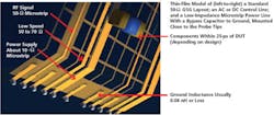
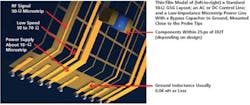
With a wide solid ground plane and a narrower conductor trace, well-controlled 50-? impedances can be maintained from the bond pad to the test equipment to provide the degree of signal integrity needed for full functional tests. In addition, if required, small-footprint surface-mount technology (SMT) components such as bypass capacitors or thin film inductors can be integrated into the membrane design along the active traces.
Components can either be on attach pads adjacent to the trace or, in space-constrained situations, the component can be integrated directly in line with the trace. The capability to mount bypass capacitors very close to the probe tip helps to lower parasitics and provides additional control over signal integrity from the DUT interface through the transmission line.
Figure 1 shows an example of low-impedance power supplies with integrated bypass capacitors. The low-inductance power and ground contacts and controlled impedance lines provide electrical performance that is consistently better than conventional mechanical needle card solutions. In addition, these electrical characteristics degrade signals less than most available IC packages and allow full functional and at-speed testing across a range of device designs.
The physical and electrical interface with the DUT is accomplished through an array of probe tips formed at the ends of the traces on the membrane. Because all of the probe tips are held in a fixed relationship with each other, they maintain consistent alignment and planarity over a greater number of touchdowns, providing a much longer life and reduced cost of ownership compared to conventional probes. The probe-tip movement at the bond-pad contact point also provides a microscrubbing action with consistent contact resistance and significantly reduces pad damage while minimizing the risk of damage to the DUT (Figure 2).
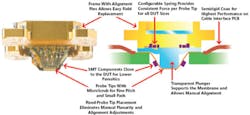
In addition to providing more accurate and consistent test results, the capability to minimize scrub also helps eliminate particulates, reducing maintenance requirements and extending the time between cleaning cycles. Because individual probes are locked in consistent alignment with each other, the need for periodic realignment of individual probes is eliminated. These factors, combined with the capability to quickly change the entire probe core in the field while maintaining consistent positioning and fixed alignment, mean higher uptime and machine utilization with lower maintenance expense and total cost of ownership.
Implementation Examples
There are some specific test challenges in which membrane probe technology is helping semiconductor manufacturers overcome the limitations of conventional probes, providing more accurate and consistent testing as well as improving production throughput and costs.
Waffle Grid Pads
Waffle grid pads or other intrametal layer pads pose particular challenges for conventional probing, especially as dimensions become smaller, both for the pads themselves and the dielectric oxide layers between the pads. For test steps required after completion of the chemical-mechanical polishing (CMP) process, it is critical that the amount of probe scrub be confined to the surface of the pads. If the scrub pushes over into the surrounding oxide, it could damage the device and create problems for subsequent processing steps.
It�s also important that all of the probe tips make consistent simultaneous contact with all of the pads. Because conventional needle probes exhibit much larger scrub patterns and more variation in probe-to-probe alignment, they can become problematic for smaller devices.
Figure 3 shows a side-by-side comparison of membrane scrub patterns and conventional probe scrub marks on a waffle grid pad.
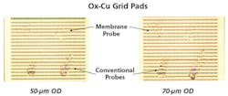
Probe alignment for testing also is very straightforward. All the probe tips in the membrane are locked together in a pattern that precisely matches the device�s pad configuration. As long as the probe is aligned properly while centered on the die, it will reliably touch down precisely in the center of all other pads on devices across the wafer.
Parametric Testing
Parametric testing of new designs requires touching down on smaller pads located within narrower streets, and manufacturers are finding that membrane probes provide an advantage. Until recently, conventional probes have been sufficient for most parametric tests. However, with RF becoming more significant, low-K dielectrics, finer pitch dimensions, and a growing need to test on soft copper pads, manufacturers are bumping up against some of the inherent limitations of needle probe solutions.
In addition, the lower particle generation from smaller, more controlled scrub patterns allows the same probe card and probe station to be used for both copper and aluminum pads. The minimally invasive scrub patterns and controlled contact pressures with membrane probes help to avoid cross-contamination when moving from differing pad materials, requiring only a relatively simple cleaning step in between.
With the same low-maintenance membrane probes remaining in place across multiple test operations, test-equipment utilization can be improved for greater overall production throughput.
KGD and SIP Testing
KGD and system-in-package (SIP) testing are other areas where membrane probe technology is being deployed. Complete and accurate KGD testing is vital for the success of high-yield SIP programs in which the functionality of each die must be verified at the wafer level to avoid the high costs of scrapping products downstream after the die have been separated, stacked, and assembled. This is of particular interest in RF applications or with devices using solder ball arrays.
By improving the reliability, consistency, and maintainability of probing solutions, KGD and SIP programs can better achieve the production-level goals of higher integration at lower overall costs. With conventional probes, wafer-level testing efficiency can quickly be degraded as a result of individual probes that become misaligned or bent or have other coplanarity problems that cause them to lift off of the target pads. In contrast, the fixed probe-to-probe alignment and flexible tension of membrane designs consistently contact pads across the entire wafer while maintaining simultaneous tip contacts during each test pass.
Empirical testing comparing the contact resistance vs. number of touchdowns has indicated that cantilever needle probe cards consistently show higher contact resistance and variation when compared to membrane probes. The difference becomes even greater when tracked across time and temperature variations.
Hitting every pad in the same spot each time and assuring consistent electrical characteristics from the pads to the test equipment are critical so that wafer-level testing can provide higher KGD yields with fewer false negatives. This helps to minimize unnecessary scrap costs at both the wafer-state and downstream assembly points.
Summary
While membrane probe technology is not necessarily the right solution for all high-speed semiconductor test scenarios, it has become an important alternative for a growing number of situations. It is ideal for those requiring consistent pad-to-pad alignment, controlled scrub patterns, minimal damage risk to the DUT, and highly repeatable electrical characteristics from the DUT to the test equipment.
As semiconductor devices continue to get smaller, faster, and more highly integrated, the need for accurate full functionality testing at the wafer level is becoming increasingly important. Membrane probe technology provides higher throughput for wafer-level tests while avoiding damage to the wafer-state devices and improving yields for downstream packaging. It will play a key role for enabling volume production of next-generation mobile wireless, video, and hand-held products that depend on RF integration, KGD, and advanced multichip designs.
About the Author
Bruce Virell is senior product marketing manager at Cascade Microtech where he is responsible for strategic and tactical product marketing plans. He has more than 17 years experience in product marketing and business development at leading companies including Mentor Graphics, Credence Systems, and Tektronix. Mr. Virell obtained a bachelor�s degree in business and marketing with engineering credits toward a bachelor�s of science degree from the University of Portland. Cascade Microtech, 9100 SW Gemini Dr., Beaverton, OR 97008, 503-601-1969, e-mail: [email protected]
February 2007
About the Author
Comment About the Article
To join the conversation, and become an exclusive member of Electronic Design, create an account today!

Leaders relevant to this article: