Estimating Emissions From Your Printed Circuit Board
Few, if any products use the hand-wired methods of the past. PCBs are the preferred technique to make that product as small and attractive as possible.
The Effects of the Need for Speed
Higher performance products can generate EMI that can affect the operation of other electronic equipment. Regulatory agencies, such as the Federal Communications Commission (FCC) and the European Union (EU) have set limits on how much EMI your equipment can radiate.
One form of this is differential-mode radiation. Any current flowing in a loop will produce a magnetic field. If that current is AC and a second loop is in that magnetic field, the second loop will have a current flowing in it too. The current in the second loop is proportional to how much of the field is coupled to it and the current in the first loop.
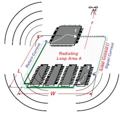
Figure 1a shows current flowing in a single circuit path on a PCB. Radio frequency EMI fields are emitted by the circuit loop and measured by an antenna at a distance. The strength of that EMI field at the antenna is:
To evaluate equation 1, perform a calculation of just one loop on the PCB. In this example, the circuit is wholly on one surface of the circuit board. The signal current flows out of IC 1 and goes into IC 2.
The current isn�t going to just stop there. It has to return to the source (IC 1).
So current flows through IC 2 out its ground pin, along the return current trace, and into the ground pin of IC 1. The signal current path and the return current path form a loop. This is the loop that behaves like a transmitting antenna.
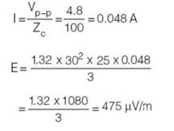
The EMI field strength can be calculated. For example,
where: f = 30 MHz
Vp-p = VOH � VOL = 5V � 0.2V
= 4.8Vp-p
Zc = 100 Ohms
r = 3 m
L = 5 cm
W = 5 cm
A = L � W = 5 cm � 5 cm = 25 cm2
This is only for the fundamental frequency. Digital signals are trapezoidal in shape with fast rise and fall times. According to the Fourier series and actual experience, trapezoidal wave shapes have higher frequency harmonics that add to the EMI field.
In addition, we calculated only one circuit loop. To be thorough, all circuit loops would have to be calculated�a rather daunting task that is not normally necessary. Typically, it�s only the circuits with the highest frequencies, currents and voltages, or fastest rise times that cause emission problems. The circuits that would be most suspect are the clock, high-speed data lines such as LSB data or address bus loops, and the IC power decoupling capacitor loops. Those decoupling capacitors supply the peak currents needed during IC switching time.
From equation 1, emissions from a circuit are directly proportional to the area of the loop and the amount of current flowing in it. The bigger the loop and the higher the current flowing in it, the more emissions that will be present. In addition, these emissions also are proportional to the square of the frequency. Therefore, don�t use an operating frequency any higher than is necessary to do the job. The good news is that the farther the measuring antenna is located away from the circuit, the lower the measured emissions. Unfortunately, that distance is set by the FCC.
Reducing the Loop Area
So what can the circuit designer do? Frequency generally is a function of the product�s performance. The higher the frequency, the better the performance and the higher the emissions potential. Loop current, to a large extent, depends on the device technology, the loads, and the operating frequency. Faster devices with higher peak currents produce higher emissions.
PCB layout is the best control over loop area, and smaller loops are better. Attention to detail in the layout will help minimize emissions radiating from the PCB.
The PCB layout must be designed to keep high-speed loop areas small. Working with the CAD operator is necessary. The key item for low emissions is to reduce the size of any high-frequency or high-speed loop.
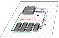
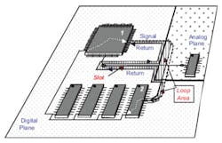
What would happen if a ground plane were added to this PCB such as shown in Figure 1b? For a ground plane at frequencies higher than 10 MHz, the return current will follow the same path as the signal current. This is because the path under the signal current is the lowest impedance path. In this case, the length of the signal path is the length of the loop and the width of the loop is the thickness of the PCB layer. The loop area is much smaller than without a ground plane.
For the circuit in Figure 1b, the loop width now is 0.15 cm compared to 5.0 cm in Figure 1a. Using the same length dimension of 5.0 cm, there is a 32 times improvement in the EMI performance for this PCB.
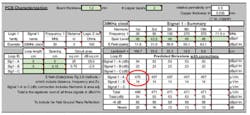
To confirm these numbers, Figure 2 is an application used in the author�s seminars showing these calculated values for some significant harmonic frequencies.1 The red circle highlights fundamental frequency results in �V/m for the two different loop areas.
Things to Watch for in the Ground Plane
The PCB ground plane is recommended in most books on EMI design.2 If the circuit is operating at frequencies above 10 MHz, it most likely will need a ground plane.
After a PCB layout is complete, it isn�t unusual to need an extra circuit or trace on the board. It could be because of a glitch found in the circuit or a new marketing or manufacturing requirement that has to be put into the product. Even on a multilayer board, often there is little room for adding traces without ripping up significant areas of the layout. Be careful when adding new traces to the ground plane.
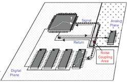
Figure 3 shows the effect of a hastily added analog circuit on a PCB. The new circuit fits easily into the layout, but may have caused an emissions problem that won�t be found until regulatory testing. The trace in the ground plane broke the return current path. Return current from IC 2 no longer can follow under the signal current path and now has to find the next easiest path back to IC 1. The circuit loop has now become larger and emissions from that loop and any other similar loops will increase proportionately.
Unintended Slots
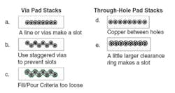
Even with the most diligent layout, slots can form in the ground plane. Figure 4 shows some of these conditions.
The normal desire is to put vias in a row. If the vias are close enough, all of the ground-plane copper is removed between them. A slot is formed, and current flow on the plane is blocked in that area.
If close spacing is needed, copper still can be between the vias if they are staggered as in Figure 4b. Even if the copper is only 0.127-mm wide, it still has a lower impedance than an open circuit.
Second, through-hole components need holes drilled through the PCB which behave like vias with larger holes. In addition, the holes can�t be staggered.
When selecting components for the layout, consider the pad stack for each pin. A pad stack includes all the details for that particular pin on the component. These details include the hole, the copper pads, and clearance ring for each layer. If the clearance ring for the copper pad is too large as shown in Figure 4e, the ground plane copper is removed between the pins, which is the same situation as when the vias are too close together.
Noise Coupling
In addition to the larger loop area when a digital trace is routed over an unrelated plane, other noise coupling can occur. In Figure 5, the area on the analog plane surrounded by the digital trace and the mutually common edge of the analog plane form a conductive path under the digital current loop. The magnetic field from the signal current path and its return current can couple digital noise into the analog ground plane and any circuits under that loop.
The optimum board layout requires careful planning to address conflicting requirements such as component density, heat sinking, mechanical mounting areas, and cost restrictions that may limit construction to only two layers. In addition, the best layout in terms of EMI performance will provide short, direct return current paths.
References
1. Swanberg, R., �PCB Emissions Prediction Workbook, V3.2,� used in D.L.S. �Controlling Emissions by Your Design� seminars, D.L.S. Electronic Systems, 2005 � 2007.
2. Mardiguian, M., Controlling Radiated Emissions by Design, Kluwer Academic Publishers, 2001.
About the Author
Roger Swanberg is a senior EMC engineer, instructor, and NARTE certified EMC Engineer at D.L.S. Electronic Systems. He is a graduate of the Illinois Institute of Technology and has held various positions in the electrical engineering field for more than 40 years. As electronics design and EMC engineer, Mr. Swanberg worked for Motorola Consumer Products and Zenith Radio, Nuvatec Design Consulting, USRobotics, and Motorola Lightning and Motorola Cellular. He presently is vice-chairman for the IEEE EMC Society. D.L.S. Electronic Systems, 1250 Peterson Dr., Wheeling, IL 60090, e-mail: [email protected], www.dlsemc.com
March 2007
About the Author
Voice Your Opinion!
To join the conversation, and become an exclusive member of Electronic Design, create an account today!

Leaders relevant to this article:
