A common trend in wireless device integration, specifically transceivers, is to incorporate the analog-to-digital converters (ADCs) and digital-to-analog converters (DACs) into a single IC or module. In cellular communications, this has given way to a new design standard called Dig-RF.1
Providing a production test solution for transceivers that have been historically classified purely in the RF or analog realm now also must be integrated into a tester with a larger amount of digital capability. Today�s ATE must face new challenges in providing test solutions for Dig-RF transceivers, which require high-speed digital data pins as well as modulated RF capabilities.
While meeting the technical demands, the test equipment also has to minimize the cost added to these devices. This is accomplished by providing shorter test times as well as keeping capital acquisition costs low.
Dig-RF devices demand processing-intensive demodulation measurements at the system level rather than at the design block. Traditionally in ATE, functional testing of devices with a large amount of digital content requires that the digital bits contained in the data to be transmitted and received be known. However, the digital data for a Dig-RF device is a nondeterministic data stream, requiring the demodulation of a signal that is independent of the RF test system.
Increasing Demands on the RF Tester
RF device testers have evolved from being a purely analog signal analyzer. Because of the implementation of digital modulation techniques, the days of testing RF device linearity such as third-order intercept, compression, and harmonic distortion have changed into wider IF bandwidth requirements.
Some examples of linearity tests that require this wider IF bandwidth are adjacent channel power ratio (ACPR) and output spectral mask testing. These tests now are routinely measured in today�s 3G cellular devices and wireless LAN devices in the production environment. This has pushed the design of RF testers to provide an environment with a low noise floor as well as a high spurious-free dynamic range (SFDR), a metric of the tester�s linearity.
In addition, these devices are further required to perform more system-level tests to measure the quality of the modulated signal, such as error vector magnitude (EVM). In EVM testing, the RF test equipment not only needs to adhere to all of the noise and linearity requirements, but it also must contain a low phase noise to successfully test EVM reliably in production.
Analog Transceiver Testing
A baseband signal would be provided to an analog transceiver from an analog baseband output of the RF tester. This is a very common requirement today. The device then up-converts this baseband-modulated signal to an RF frequency.
A DAC in the tester provides a baseband I/Q signal to successfully make RF measurements for these devices. At this point, the signal integrity is a function of the bit resolution of the DAC as well as noise power.
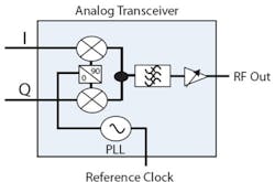
Figure 1 shows the transmitter section of a typical analog transceiver. This transceiver requires a reference clock, which it uses to produce the local oscillator frequency that internally modulates the baseband signal onto a carrier. The tester then would acquire the signal, demodulate it, and test the desired parameters.
Figure 1. Analog Transceiver Test Signal Flow
In the case of a Dig-RF transmitter chain, the DAC supplying the analog signal is internal to the device. The device uses parallel or serial digital input/output signals, which are provided and acquired by the tester. The most common configuration uses a serial implementation of the digital data since the end-device package needs fewer signal pins.
The digital bits represent an analog signal by using a pulse code modulation/demodulation scheme. The signal integrity is a function of the number of bits used in this scheme: the greater the number of bits, the lower the quantization error of the device.
Currently, this type of architecture is used for high data rate signals such as devices that transmit wireless LAN modulations. Data, in this implementation, can be clocked at a rate as low as 20 MHz for an 802.11A signal. The transmitter of this type of device has the DAC built into the chip.
For a W-CDMA signal with an 8-b resolution, the minimum sampling frequency for clocking the digital stream into the device would be 3.84 MHz for eight parallel digital pins, or the bit period has to be approximately 260.5 ns. A digital signal of 3.84 MHz can be provided by many digital sources/samplers.
Parallel-Pin Digital Input Devices
The pin-count on a device designed with this architecture can increase dramatically with parallel bits in the baseband digital input. There are many reasons for minimizing the pin-count in today�s transceivers; for example, to integrate more functionality into smaller available spaces. This is a major reason for a large interest in creating a Dig-RF standard.
The Dig-RF standard specifies that at least one pin shall be used for transmitting the digital baseband data. A common configuration implemented today uses four pins total to transmit the I and Q input and output channels (one pin for each). If this topology is used to transmit an 8-b resolution signal, it yields an architecture that looks like the device in Figure 2.
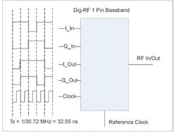
Since one pin is used for each data path, a single digital pin now must transmit this 8-b data serially into the Dig-RF device to have the 8-b resolution. This is accomplished by clocking the data at a rate that is eight times faster than it was before for the same bit rate. If I and Q share the same pin in a multiplexed architecture, the data would have to be clocked into the device at a speed 16 times faster than the original 8-b parallel device.
The RF tester has to be able to transmit, receive, and analyze this digital baseband data. As can be seen in Figure 2, for a W-CDMA-type device, the clocking rate now is 30.72 Hz; for a WLAN device, the clocking would be implemented at a minimum of 160 MHz.
With the implementation of Dig-RF in these next-generation devices, the RF tester now has to be able to achieve digital source and capture speeds that are beyond most low-cost ATE. In addition, the traditional digital architecture of an ATE digital pin is not optimized for the types of tests being performed. Nondeterministic digital data requires digital signal processing (DSP) rather than traditional pass or fail test techniques.
These requirements reach beyond what typically is considered an RF tester and more into the domain of a higher-cost system-on-a-chip (SOC) tester. The device remains a very cost-sensitive component in a wireless system, and replacing the analog interface on the chip with a digital interface should not demand additional test cost to the IC manufacturer. A new test methodology is required to keep these types of devices tested in production on low-cost ATE.
Testing Dig-RF Devices
Since these RF devices are highly integrated, many of the RF measurements that once were implemented in a test procedure now cannot be done due to the lack of access to different modules inside the device. This assumes analog test modes are not provided by the device manufacturer, but many design-for-test (DFT) techniques can be used to allow traditional test techniques on next-generation devices.
For example, a test that commonly is implemented for many purely RF devices is the 1-dB compression point (P1dB). By definition, P1dB is the point at which the gain of the device is reduced by 1 dB as a function of the input power due to nonlinearity. The RF portion of the device in Dig-RF chips is so far into the transmission chain that the RF signal cannot be injected by the tester into the RF portion of the chain.
Traditional gain and linearity tests still can be performed; however, the data can only be determined for the entire signal path from RF to digital. In these types of devices, EVM and output spectral mask are desired to test the RF chain. These tools allow the device manufacturer to see how the entire chain of transmit or receive blocks inside the device performs without having to test each block individually.
EVM is highly dependant on many parameters that once were tested separately. If the phase noise of a device is high, an EVM test will detect it. If a device is nonlinear, EVM and spectral mask will detect this. Many of the parameters that once had to be tested individually now can be implemented by a single test, considerably reducing test time and cost.
The RF Tester as a Receiver
Due to the evolution of RF measurements pushed by highly integrated devices, Credence�s Modulated Vector Network Analyzer (MVNA�) RF subsystem has evolved into a low-noise receiver that can extract the symbols in a particular digital modulation. For example, the RF test system must be aware of training sequences in some of the digital modulation standards to provide correct time synchronization to comply with the standard. This is especially true in orthogonal frequency division multiplexing (OFDM) systems where, if the tester is not synchronized in time with a received waveform, the constellation is nearly impossible to extract.
Also, many devices now are tested using an external crystal to provide the reference clock for the integrated chip to supply optimal phase noise performance. The result is that the device is not phase-locked to the ATE system, which can cause a nondeterministic amount of frequency difference between the device and the tester.
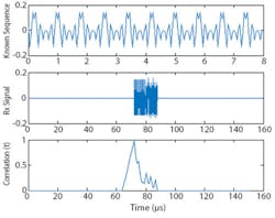
Top: 802.11A short training sequence
Middle: received signal containing zeros, the short training sequence from 72 �s to 80 �s, followed by transmission data and more zeros
Bottom: correlation between the known training sequence and the received signal
Figure 3 shows how time synchronization is implemented from a received signal. For display purposes, the training sequence shown is from an 802.11A short training sequence header. For an OFDM system, the time synchronization can be implemented in the time or frequency domains. Correlation is done the following way:2
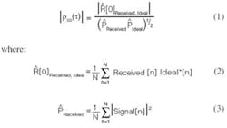
From equation 1, if a perfect match of a known sequence is found in the received signal, then the correlation will peak at 1.0. In practice, correlation will not peak at exactly 1.0 due to noise in the signal, but there always will be a distinct peak that corresponds to where the signal starts in a time series. This correlation methodology must be implemented for time synchronization to compute EVM in OFDM-type signals.
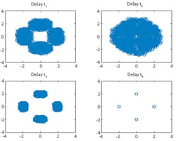
For modulations where the constellation is contained in the time domain, this correlation methodology may be used to synchronize to a known training sequence but is not always necessary for testing EVM depending on the standard. Computing EVM at different time offsets will give the user an optimal EVM measurement.
This is illustrated in Figure 4 where different time delays will accomplish different received constellation plots from the same acquisition. Due to amplification or attenuation, this received signal also would have to be scaled and rotated in phase due to the uniformly distributed random-phase addition inherited from the multiplication of the signal by the local oscillator in the up-conversion or down-conversion process.
For more complex constellation plots, there are more steps necessary to ensure proper calculation of an EVM measurement. Time-shifting a received signal can be implemented using the following property of a Fourier transform pair:3
Frequency error correction also may be incorporated into the measurement if an external crystal is used to drive the reference clock of the device. This case is going to be likely even if the test equipment and the device are clocked by the same frequency reference due to small amounts of error in the device�s PLL and fractional divider.
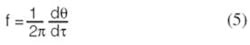
In OFDM systems, this frequency error is measured from either long or short training sequences and can be done in either the frequency or the time domain. In both time-domain and OFDM-type modulation schemes, this frequency error induces a phase rotation that has a constant first derivative. The frequency error is directly related to this derivative, and this relationship is defined as:
Once this frequency offset is found, a correction can be applied to the received signal. The time series then can be corrected by applying a frequency shift with the same value as found in equation 5 by negating the value. The time shift then would be implemented, and EVM can be accurately measured.
Testing the Dig-RF in Production
RF testers now must support the Dig-RF interface standard and the digital source and measure capabilities to test this set of next-generation devices. Since the measurement requirements are more analog in nature than traditional digital test methods, the DSP algorithms required are very similar to what usually exist in the RF subsystem of these testers.
Cost of Test
Besides being able to technically solve the test needs for manufacturers of these highly integrated devices, the cost of test also is a very important parameter. The Dig-RF standard specifies digital data rates up to 400 Mb/s. These types of digital speeds traditionally direct the consumer of an ATE system to a class of digital architecture that is focused on functional pass-or-fail testing.
Using the digital instrument in this manner is effectively using it as a capture card front end, which serves only as a medium to pass acquired data from the capture instrument to a processor for the DSP calculation. This is a very expensive use of the tester�s digital pin; the majority of the functionality of that tester pin is not being used, but the consumer is paying for it.
In addition, these ATE architectures usually are not designed to transport several hundred thousand acquired samples from the digital instrument to the processor. Doing so results in a large transfer time that directly adds to the time to test the device.
As mentioned before, the digital data in a Dig-RF system is nondeterministic. In addition, it usually is made up of highly over-sampled, unformatted sigma-delta data, a very raw format that requires decimation and finite impulse response (FIR) filtering to even perform the DSP required for a measurement such as EVM.
Credence Systems� digital baseband (DBB) instrument performs much of the complex signal processing onboard the instrument. It reduces the mathematical load and transfer time for the test system by preprocessing the data to fit the format of the Dig-RF standard. This allows acquired digital data volume to be reduced by several orders of magnitude, freeing up computer clock cycles of the RF subsystem to do other processes in parallel and speeding up test time.
The DBB instrument can be installed in the company�s existing ASL 3000RF tester. By using the MVNA RF test architecture and adding a digital source and receive instrument, the capital cost of the tester remains very competitive for Dig-RF transceivers as it is for analog transceivers.
Conclusion
As Dig-RF devices ramp up in volume, production testing of wireless devices is becoming extremely versatile and highly modular and must be ready to change quickly for the next generation of devices. Modularity of the tester instrumentation is extremely important to keep the design of the tester itself unchanged. This helps device manufacturers ramp up time to production, which is essential in winning market share, and keeps the overall cost of test low.
The ATE supplier must understand these changes and evolve as new chip designs go into production. Test engineers also must be constantly training themselves to become experts in Dig-RF devices. By providing efficient point-solutions to high-volume technologies, the cost of volume production can keep reducing as the wireless IC integration trend continues and device complexity increases.
References
1. Fogg, A., �DIG/RF Baseband/RF Digital Interface Specification, EGPRS Version 1.12,� Digital Interface Working Group, 2004.
2. Chandrasekar, V. and Bringi, V.N., Polarimetric Doppler Weather Radar, Cambridge University Press, 2001.
3. Couch, L.W. II, Digital and Analog Communications System, Fifth Edition, Prentice Hall, 1997.
About the Author
Max Seminario is a marketing applications engineer at Credence Systems. He has spent most of his career developing RF solutions ranging from telemetry and range safety design to working in the ATE industry. Mr. Seminario received a B.S.E.E. from the University of Florida and an M.S.E.E. from Colorado State University where he conducted research in the radar laboratory. Credence Systems, SDG Division, 1421 California Circle, Milpitas, CA 95035, 408-635-4300, e-mail: [email protected]
FOR MORE INFORMATION
on the Dig RF interface specification
www.rsleads.com/703ee-176
March 2007
About the Author
Comment About the Article
To join the conversation, and become an exclusive member of Electronic Design, create an account today!

Leaders relevant to this article: