Consider this scenario at a major semiconductor company: You are in charge of device testing, and marketing just delivered great news. The largest contract in the history of the company has been secured for next-generation cell phone chips. The chips are to be highly integrated to target the $20 cell phone market, and the volume potentially could be more than 1 billion devices per year. Everyone at the company is excited.
Marketing then delivers the rest of the news. Competition for the contract was incredible, and the team had to make aggressive performance and price commitments to win the business.
The chips must be integrated using 3-D packaging to achieve the size, performance, and cost requirements. The IC design, wafer front-end, and the test groups all are asked to help drive overall costs down. In particular, the test group needs to reduce the cost of test by 50% to meet profitability targets.
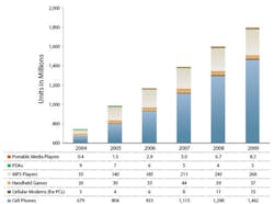
This scenario illustrates the potential benefits and pitfalls for device manufacturers associated with the paradigm shift in the logic device market driven by consumer demand for electronic devices such as hand-held phones and MP3 players (Figure 1). This shift includes very high volumes, high functional integration, high performance, and extreme pressures on the average selling prices of devices. At the same time, consumers dictate a shrinking window of opportunity for new products before the next great thing becomes popular.
Source: In-Stat, June 2006
Implications on Test
Mobilization, connectivity, and multimedia result in the need to cram ever more functionalities into smaller form factors. Consequently, new packaging technologies are needed, specifically 3-D, where multiple dies are stacked into a compact package, multiple packages are stacked on top of each other, or a mix of both are placed inside a 3-D package.
This integration makes it very difficult to perform package test cost-effectively and drive new wafer test requirements to meet known-good die (KGD) reliability requirements. These include more test insertions, testing at multiple temperatures, high-frequency testing, and wafer-level burn-in.
Device test times also are rising dramatically. Longer test times are driven by higher levels of embedded memory, higher functionality, higher quality requirements, and the need to move more tests to wafer sort.
It is not uncommon to see logic device test times reach tens or, in some cases, hundreds of seconds. This is a new condition that demands a reanalysis of long-held assumptions about the optimal partition of logic IC testing between wafer test and package test.
All of these new wafer-sort testing requirements render the current installed base of logic ATE inadequate to meet the challenge. It is time for a new strategic approach. Any new logic testing strategy will require higher levels of test parallelism to be effective as has been the case with memory testing over the last 10 years.
Taking our sample scenario where the test manager needs to test 1 billion devices, a simple analysis shows that some $296M in capital equipment is needed to deliver the volumes of tested devices just for wafer sort test (Table 1). This investment can be reduced dramatically by enabling x4, x8 or x16 devices tested in parallel at wafer sort.
�
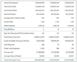
Table 1. Cost Projections of Testing a Billion Logic Devices
In addition, major benefits can be achieved by an optimal design of the test flow between wafer sort and final package test and by leveraging a strategy to speed up the device yield ramp. To achieve this, multiple factors that include the IC design, the ATE test cell, and the probe card solution must be considered. Ultimately, test-cost reduction boils down to two efforts: optimizing test flows by moving more tests to wafer probe and maximizing efficiency of wafer probe test cells.
Test-Flow Optimization
There is a critical need to change traditional test-flow approaches that were developed over the last 30 years. Significant savings can be achieved by changing the sequence of tests across the entire IC test process. The net result is to move entire tests or critical test sequences to much earlier in the test process, which usually means more wafer-level testing to support KGD quality, collecting more device performance data early in the process, and enabling higher levels of parallelism.
The best approach to develop an optimal test flow starts with a full audit of the current test-flow sequence and the criteria for selecting the specific sequence. This initial step will uncover many cases where the test sequence was selected based on assumptions that no longer are valid.
For example, a conventional assumption has been that probe testing can only be done at low frequency. This assumption no longer is valid because advancements in probe card technology now support high-speed wafer testing.
Managers must make a decision on how to partition test between wafer and package tests and where to focus energies to increase parallel testing. In the sample scenario, the need to support 3-D packaging and KGD quality as well as address yield-learning pressures dictates a wafer test-centered strategy.
However, there are other factors that drive this conclusion even in the absence of these requirements. One factor is the financial impact of assembling and packaging defective devices. This factor is critical in high-functionality ICs where yields are low and yield rates at package test are modest. In the case of 3-D packaging, one defective device will ruin the entire system.
A second and perhaps more significant factor is the difficulty in implementing high-parallel package IC test strategies. The size and structure of logic IC packages limit parallelism to just a few devices. As a result, the trend today is to focus on wafer sort for high parallelism testing.
Test-flow partitioning between wafer sort and final package test can have a dramatic impact on the cost of test. In some cases, the migration of package tests can be done over time, but the test manager must ensure that the wafer-sort solution design will support this type of optimization. Critical issues will arise if the wafer-sort solution will not support higher-speed test conditions or a wider range in test temperature conditions.
By rearranging test sequences and enhancing existing test designs with new capabilities, it is possible to eliminate entire test insertions with a dramatic impact to testing throughput. This must be done while improving or maintaining device quality.
A fresh look at the test flow can result in a 30% to 50% reduction in the cost of test by eliminating insertions or, in some cases, dramatically reducing package test. In a situation where wafer test is done even at only four times higher levels of parallelism than package test, the benefits of moving tests to the wafer level become obvious.
Increasing Test-Cell Productivity
Once the decision has been made to move more tests to the wafer, the next step is to look at ways to increase test-cell productivity. As shown in Table 1, a preliminary analysis using a test-time projection of approximately 4.5 s per touchdown, average equipment costs, a modest device yield of 70%, and typical equipment uptime shows that a x4 parallel test strategy or higher will be needed to significantly reduce the cost of test for the current generation of devices.
In the sample scenario, the test manager wants to target testing x8 devices in parallel with a backup strategy for four devices in parallel. The higher parallel strategy most likely will involve new test systems with higher test resources and more effective parallel test capabilities.
Leveraging the current installed base of systems limits him to x4 in parallel but provides a faster way to leverage current resources and determine high parallel test feasibility. In this case, having two different parallelism targets for both the current installed base of test systems and new test systems will lead to an optimal use of resources.
Selecting a preliminary target for the level of parallel test sets the stage for an effective execution program. Across the spectrum of logic ICs, parallel execution programs range from two devices to 512 devices in parallel.
The optimal target will depend on the nature and complexity of the device, the implementation of design for test (DFT) and built-in self-test (BIST), test equipment and prober capabilities, and the availability of probe card solutions. The right mix of capabilities will be determined by their availability and cost-effectiveness.
In the early days of logic testing, the fundamental nature of the IC dictated the test strategy and requirements, and wafer test was performed one device at a time. Key device parameters included the number of I/O channels, the number of device supplies, test frequencies, and the need for analog test resources such as waveform generators and digitizers and other special test resources like high-precision timing measurement systems.
Overall power requirements limited the test strategies for devices. The use of embedded memories forced the need to provide algorithmic pattern generators, and the circuit complexity drove the level of vector memory requirements.
ATE also was developed for specific logic segments. This situation has changed in the last 10 years with the deployment of more aggressive DFT and BIST implementations and the emergence of integrated system-on-a-chip (SOC) devices, which drive the need for universal ATE architectures that provide more resource flexibility and expansion.
A system-level approach now is required to cost effectively achieve higher parallelism at probe due to the range of options and trade-offs between device-centric solutions and equipment-centric solutions. Focusing only on ATE capabilities will lead to lost opportunities to leverage new developments in DFT techniques. Focusing only on DFT ignores the capability of ATE suppliers to bring more effective solutions with every new generation of test systems. An effective strategy not only considers the current capabilities of ATE, probe card solutions, and DFT/BIST tools, but also improvements and capability roadmaps.
Device-Centric Testing
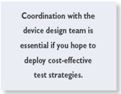
Coordination with the device design team now is essential if you hope to deploy cost-effective test strategies. In the past, DFT and design partitioning were the main focuses to improving test effectiveness in terms of fault coverage and test times.
Most traditional DFT programs concentrated on increasing observability and controllability by adding circuits. The addition of BIST focused on reducing the testing-frequency requirements. This allowed semiconductor companies to extend the lives of their test systems and meet their test requirements with lower-cost test systems. It was very effective and allowed companies to meet cost-reduction targets over the last four to eight years.
Consider this scenario. A test manager wants to coordinate with design to reduce the number of resources required to test a device as well as control the structure, pitch, and layout of the die contact points to facilitate more effective probing. Lowering the number of resources needed to test a device will allow the ATE to test high pin-count devices without major expansion in system resources.
It is possible to implement DFT and BIST to effectively test high pin-count devices via a reduced pin-count port. The aim is to reduce the amount of testing resources that do not scale easily, such as high-speed tester channels with very deep vector memory requirements. However, care must be taken to avoid creating excessively long test times or dramatically increasing the device power consumption during the testing modes.
The placement of probe pads or bumps can have a dramatic impact on the probe card because of signal routing requirements and available probe card pitches and densities. It also is important to review the circuit chemistries and sensitivities as early as possible in the process or device design phase. Pad or bump shape and composition can have a significant impact on the lifetime of the probe card and system uptime due to probe card cleaning-frequency requirements.
DFT and BIST also are critical in reducing the cost of testing very high-speed serializer/deserializer (SerDes) structures that will perform at more than 3 GHz but can be tested at much lower speeds by adding loop-back testing structures. In this case, the device is providing its own testing signals, but the ATE or probe cards need to support this test mode with signal control and conditioning.
In the long term, it will be DFT and BIST innovations that will enable very high levels of parallelism and even single touchdown to test a complete wafer for complex logic devices. For this scenario, the critical benefit will come from lowering the quantity of I/O test channels to support higher levels of parallel testing.
Current baseband cell phone chips require 200 to 300 I/O channels, and typical ATE only supports 1,024 I/O channels, consequently only accommodating three to four devices in parallel. DFT and BIST can reduce the full-function test I/O count requirements to less than 64 channels to support x16 parallel test execution.
ATE-Centric Testing
In most situations, the current installed base of ATE does not support the desired level of parallel test execution. The usual test-resource gap involves limited I/O test resources or a limited number of power supplies available for the DUT. Closing the resource gaps can be done by expanding the ATE configuration or upgrading to test modules with higher resource densities. Both alternatives involve significant technical and business trade-offs.
ATE resource expansion depends on the availability of both system expandability and expansion resources. When the system has room for expansion and the ATE vendor has the desired expansion solutions, it becomes solely a case of weighing cost vs. benefit and securing the capital dollars to enable the higher capability.
New modules could be developed by the ATE vendor or third-party companies, but most efforts typically take 18 to 30 months to execute. Proprietary system architectures and undocumented specifications make it difficult but not impossible for third-party companies to develop effective solutions.
In the case of older ATE, the original vendors may not have the engineering capability or desire to develop new test modules. In such cases, third-party vendors could be the only option to close functional gaps.
Some ATE upgrades require fundamental changes to the system to support higher levels of capability. This could involve wholesale replacement of entire subsystems to remove the original limitations. These upgrades have significant price tags and need to be evaluated against other options and the feasibility of using current ATE resources for other devices.
In some cases, the semiconductor company could sell the ATE to generate capital toward the purchase of new systems with lower resource limitations. The optimal solution usually involves some expansion of resources to close functional gaps or the repositioning of current systems to perform lower levels of parallelism or support wafer-level burn-in strategies where the stress cycles are very long. Such a solution also is impacted by the capability to add significant test resources around the probe card.
Probe Card-Centric Testing
The opportunity to close functional test resource gaps by adding resources on or around the probe card is driven by cost-effectiveness, the availability of new silicon-based solutions, and performance advantages. The idea is to supplement the test system resources to achieve higher levels of parallelism at a minimum cost, which is an effective way to extend the economic life of the installed ATE base.
Probe card-centric solutions can increase the number of test channels or the number of device power supplies with supporting circuitry mounted directly on the probe card or implemented on daughter cards. Care must be taken to deliver the right signal fidelity and the needed support for resource calibration and diagnostics. This approach is opportunistic but can have a significant impact on the cost of test when the installed base is very large.
New IC technology and higher levels of integration make it possible to provide significant test resources on the probe card, such as device supplies, digital channels, and analog test modules, with suitable performance. This capability can dramatically remove traditional test limitations and turn an obsolete tester into a valuable resource.
Probe card-based supplementary test resources also have the advantage of close proximity to the DUT. This usually is important when signal quality and fidelity make a difference.
In some cases, it is possible to add device test circuitry only a few millimeters from the DUT. This can be critical for analog circuits, RF test structures, and circuits needed to support high-speed loop-back solutions.
Effective probe card solutions are optimized to achieve specific results based on higher levels of test parallelism, improved device yields, and more effective test partitioning. These elements will determine the fundamental cost-effectiveness of the test strategy.
Care must be taken to fully consider all these factors when developing probe card solutions. Besides supporting critical test circuitry, probe cards can be designed to support high-speed testing and cold and hot temperature testing. Such advanced technology probe cards with precision contact capability can be critical in enabling not only more effective test partitioning but also smaller die sizes and faster yield ramps by providing better signal fidelity.
Developing the best test strategy requires a comprehensive perspective on the entire process in partnership with multiple functionalities. Early partnership and collaboration with strategic suppliers become critical for a successful implementation. It is easy to miss valuable cost-saving opportunities early in the device design cycle when decisions are made that impact testability and parallel execution for the life of the IC.
Conclusion
The logic IC world is experiencing a paradigm shift that requires a new approach to wafer test. Higher device functionality and complexity place greater needs on testing while the consumer demand places much greater pressure on test costs.
However, the relatively large device volumes create a great opportunity for innovative new approaches to achieve test cost savings. This paradigm shift has made cost-effective testing a strategic requirement. Higher levels of wafer test parallelism will provide the core cost-of-test savings, but in some cases, higher yields and test-flow optimization can provide dramatic benefits.
Probe card solutions that extend the life of existing ATE assets have tremendous financial leverage. To be effective, these solutions will need to be part of a system-level approach that involves closer collaboration among the ATE suppliers, the probe card suppliers, and device designers.
About the Author
Sergio Perez is vice president, SOC marketing, at FormFactor and has more than 20 years of experience in the semiconductor industry. Prior to joining FormFactor, he was vice president, business development at Advantest America and held marketing and management positions at Comdisco Electronics, Teradyne, Megatest, Schlumberger, and Aerojet Electrosystems. Mr. Perez received a bachelor�s degree in engineering from Harvey Mudd College and an M.B.A. from Harvard Business School. FormFactor, 7005 Southfront Rd., Livermore, CA 94551, 925-290-4000, e-mail: sperez@
formfactor.com
July 2007
About the Author
Comment About the Article
To join the conversation, and become an exclusive member of Electronic Design, create an account today!

Leaders relevant to this article: