Advances in Test Program Automation
Founded in 1984, Atmel designs and manufactures advanced semiconductors including logic, nonvolatile memory, and mixed-signal and RF integrated circuits using advanced wafer processes such as BiCMOS, CMOS, and silicon germanium (SiGe) technologies. Our division in Rousset, France, focuses on cell-based ASICs and application-specific standard products (ASSPs).
The ASIC product range addresses medium- and high-volume applications where optimum performance is required at the lowest unit cost. The ASSPs are geared toward the consumer multimedia and communications markets.
Fundamentally, both product lines are advanced SOC solutions incorporating sophisticated intellectual property (IP). Some of the primary IP blocks available are nonvolatile memory such as flash and EEPROM, embedded RAM, processor cores such as ARM and AVR, analog IP blocks such as PLLs and audio and video converters, and I/O cell blocks with programmable pull-ups/pull-downs and bus holders.
Our business model necessitates the design and manufacture of very complex devices at very competitive prices. This combination drives a requirement to aggressively cap the overall cost of test including test program development.
Atmel created an automated test program development flow to accomplish these seemingly contradictory objectives. Our automatic test program generation (ATPG) system traces its lineage back to the acquisition of the European Silicon Structure more than 10 years ago. Our early efforts in ATPG produced test programs for the Credence Quartet and ITS 9000 tester family and the Nextest Maverick and were relatively successful.
Unfortunately, as the complexity of our devices continued to track Moore�s law, we needed to integrate newer, more powerful platforms into our ATPG system. Extending our automated flow to suit the Sapphire platform met this challenge and resulted in enhanced capabilities.
Test Program Generator Overview
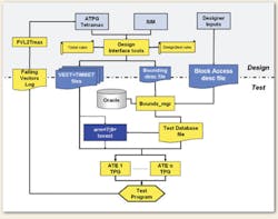
Our test program generator (TPG) bridges between the design world and the test world as shown in Figure 1. We use standard EDA ATPG tools such as Tetramax or FastScan, depending on the requirements of the different design groups.

Figure 1. ATPG Structure
A generic design interface tools (DIT) suite was developed within our design-flow group. The actions of these tools are moderated by a set of files created by test engineering that defines the specific tester constraints and design-to-test rules. Together, these files specify the authorized timing formats, initial pin states, strobe placements, and test rate limitations.
Another input to the flow is provided by the designer through a Block Access Descriptor file which describes the available ASIC library blocks such as processors or memory. Using this description, the TPG for the target ATE can generate special program modules and patterns for some of the large IP blocks available. These include an ARM core with full test insertion or nonvolatile memory patterns and flow using a standard serial test interface port that is part of the design library.
Based on the inputs given, the DIT produces a set of files for downstream use by the target TPG:
� A collection of test vector files, together with timing information using an internal data representation.
� A bounding description file which defines the I/O cells being used and their electrical parameters extracted from SPICE simulations performed by the design group.
� The block access description file created by the designer.
In cases where special cores are instantiated in the design, such as an ARM core, additional predefined vectors are linked into the VECT files for processing.
DFT insertion and driving the creation of test vectors through ATPG are the design group�s responsibilities. Very high fault coverage goals have been set for DFT.
The bounding description and block access description files are used as inputs to the Bounds manager. Information about the device package type and die pads is extracted from a database written in Oracle and used for load-board and probe-card build instructions. The Bounds manager outputs the test sequences needed by the I/O cell technology together with the test limits to be applied taking into account factors such as temperature and VDD level.
The Test Database file together with the VECT + TIMSET files then are sent to the target TPG to generate the actual test-program source code.
Anatomy of the Test Program
The target TPG module actually is capable of generating multiple versions of a device test program based on where in the development phase the device is. This is a fundamental advantage of our automated test program development methodology.
Typically, the test program would comprise the following:
� Load Board Tests Executed Once After Program Installation
� Opens and Shorts Tests
� Gross Idd Tests
� Device Trimming Procedures
� Memory Tests
� Functional and Structural Tests
� Analog Tests
� Idd Standby Tests
� Vol and Voh Tests
� Leakage Tests
These automatically generated analog tests are primarily simple static tests for most of the simple analog cell structures such as op-amps, band-gap references, and simple DAC/ADC and used primarily in prototype debug because they would be too slow for production use. For leading-edge custom mixed-signal cells, the test code needs to be added by a test engineer. Given the current technology available, fully automated tests for advanced mixed-signal cores still is a subject of intense research in academia.
Many of the test routines are written generically and stored in external libraries accessible to the test programs. They perform various functions normally associated with all test programs such as the test session program (TSP) interface which includes prober/handler data and lot information.
Different versions of the test programs are generated by our tools during the device life cycle from the same set of inputs:
� First silicon test program, usually carrying many scan and functional test vectors, created by ATPG and the designers for silicon debug purposes.
� Production test programs optimized for wafer sort package test.
� Device characterization test program, suitable for use in yield enhancement programs and failure analysis lab work. This version is the most sophisticated kind of test program. It is geared for use by a product engineer and includes features for bit mapping and special routines for interacting with some of the test parameters.
To speed up first-silicon prototype turnaround time, we have created a special per package loadboard with jumper fields that allow the operator to patch in the needed tester resources such as power supplies to the appropriate DUT pins. This can save weeks in the fabrication of a custom loadboard. The TPG produces loadboard patch instructions for the operator, correct pin definition statements, and loadboard diagnostic tests to ensure correctness.
Most of the products have multiple package delivery mechanisms plus wafer sort. This leads to multiple test programs and test vector files to accommodate the different tester pinouts. To reduce this logistics complexity, we try to leverage as much capability as is available from the tester in terms of pin scrambling and pin definition switching.
Special Debugging Tools
Special routines included as part of the test program are meant to facilitate the rapid bring-up of a new device test program during the prototyping phase. These tools are:
Race Time Checker
Race time checker allows timing edges to be easily shifted in time during tests (Figure 2). With this tool, we can catch all remaining simulation timing race conditions that may be present at prototype test. The tool also expedites the transfer of test programs between platforms such as from the characterization to a production system that may have additional timing restrictions.
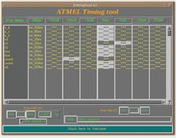
Figure 2. Timing Race Checker
Fail Vector Listing
All test programs can generate a listing of failing vectors per pattern in a format suitable for the designer. The designer can use this information to create additional ATPG vectors to more precisely localize the physical defect.
First-Fail-Per-Pin Listing
The goal of this tool is to give the designer the maximum information about the failing functional pattern.
Extending the Automated Flow
As our devices grew more complex, we needed to upgrade our test capability to encompass a new generation of ATE. After a thorough evaluation, we chose the Credence Sapphire platform and XTOS software because it provided the cost/performance and long-term scalability we needed.
The Sapphire system has a totally different hardware and software architecture than our previous testers. We had to rethink how to integrate it into our automated flow, but the end result was a more powerful and easier to maintain flow than was previously possible.
Figure 3 illustrates some of the new tools developed for Sapphire. Included are the following:
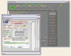
Figure 3. Production Interface Tools
Object-Oriented Programming
XTOS incorporates an object-oriented programming language (Java) in which to write test templates. Templates come with the system, or new ones can be created and made available in a library. The Sapphire TPG makes extensive use of this capability.
XML Data Structures
The test program data values are kept separate from the test templates in XML blocks. XML is an industry-standard mark-up language derived from the older HTML used in websites. XML blocks are very easy to parse and create with computer tools. With XML, we can develop our own highly customized data structures such as for the TSP without totally changing the existing test programs or TPG.
The separation of test procedures from the data they require resulted in considerable simplification of the TSP code generation that was needed for Sapphire.
Scripting Capability
XTOS includes Python scripting capability. Python is another industry standard having more capabilities than the older PERL. Anything that an XTOS test program can do to control the tester hardware or terminal I/O can be controlled from a Python script. This allowed us to develop very comprehensive characterization test suites requiring a combination of test programs and scripts through minimum operator interaction�a big boost in total possible automation.
STIL
The native vector source language used by XTOS is standard test interface language (STIL), an IEEE standard. STIL is very similar in capability to our VECT + TIMSET format. Since the new ATPG tools available today can output STIL, we have converted our vectors and timing formats to use STIL and save on the maintenance of VECT + TIMSET for new testers.
NAME MAPs
In XTOS, the device pin-to-tester channel assignment is defined through a NAME MAP data structure. By itself, this is not unusual. The vectors are dynamically loaded to the tester memory based on the NAME MAP, and multiple NAME MAPs can be defined in the test program. In effect, the NAME MAP that is conditionally selected determines how the vectors will be loaded.
In the past, we had to generate and keep multiple versions of the patterns for the same device that could include a wafer sort pattern set and unique pattern sets per package type. With hundreds of active device types in manufacturing, keeping track of all these patterns was a logistics challenge. With XTOS, we only need to create one pattern set and let XTOS handle the DUT-to-tester channel mapping.
The concept of NAME MAP also is central to developing programs for multisite testing needed on many devices to lower the cost of test. For multisite test, the TPG creates a NAME MAP that replicates the DUT-to-tester channel connections as many times as there are test sites. During testing, extensive amounts of data are collected for off-line analysis using the industry-standard STDF format. Figure 4 is an example of some of the types of analysis we can perform.
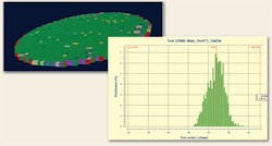
Figure 4. Analysis Plots From Wafer Test Results
Conclusions
Our automated methodology has evolved to handle our most complex devices and given us a very real economic advantage in cost of test. As a result, we currently generate approximately 400 different test programs per year, our test engineering staff of approximately 10 engineers supports the run rate, and on average, it takes around two hours of tester time during first silicon debug to have a working program and produce meaningful data for the designers.
Extending our flow to the Credence Sapphire system resulted in an even more powerful implementation of our automated flow than was previously possible. This was a direct result of the architecture and the capabilities brought by XTOS software. For this reason, the Sapphire platform has become our system of choice for silicon prototype debug and characterization.
About the Author
Christian Bonnin is the test engineering manager in the ASIC RFO Division of Atmel. Prior to joining the company, he worked in test engineering at the European Silicon Structure and Schlumberger R&D in Clamart, France. Mr. Bonnin graduated from the Ecole Centrale Electronique in Paris. Atmel Rousset, Zone Industrielle, 13106 ROUSSET, France, +33 4 42 53 60 47, e-mail: [email protected]
FOR MORE INFORMATION
on the Sapphire Test System
www.rsleads.com/707ee-184
July 2007
About the Author
Comment About the Article
To join the conversation, and become an exclusive member of Electronic Design, create an account today!

Leaders relevant to this article: