2-4-6-8 What You Gonna’ Simulate?
As any sports fan knows, you get prognostications from the pundits. For actual results, you play the game. Regardless of how obvious an outcome may be, until the game is played, the predicted result can only be an estimate based on experience and hunches.
So too, circuit design isn’t really completed until thousands of the same circuit have been built that all perform to the specification. Nevertheless, in contrast to sports, circuits can be precisely modeled, which provides a very good chance of first-time design success. To become more familiar with typical capabilities, we decided to evaluate a modern circuit simulation program.
The National Instruments (NI) Circuit Design Suite 11.0 includes both Multisim™ circuit simulation and Utiliboard™ PCB layout applications. We chose to explore the circuit simulation capabilities available in an evaluation version of Multisim downloaded from http://digital.ni.com/express.nsf/bycode/downloadmultisim?opendocument&lang=en&node=seminar_US.
Multisim is promoted as a teaching tool, and its advantages are easy to see. Instead of directly interacting with SPICE, you are presented with a number of abstracted tools that keep the focus on your circuit design, not on the intricacies of simulation. Of course, you don’t have to be a student to appreciate Multisim’s ease of use and comprehensive features.
In addition to extensive component and AC/DC source libraries from which the circuits are constructed, several generic and manufacturer-specific test tools also are provided. Once a representative schematic is assembled, you can attach a virtual multimeter to various points to check DC bias levels. Or, you can probe circuit nodes with a virtual oscilloscope to help understand phase relationships.
From a teaching perspective, having both Tektronix and Agilent Technologies scopes available for every student in a course is a big deal. It’s especially important that students are exposed to more than one brand of control interface although often this is impractical with real instruments. With Multisim, the scope simulations are sufficiently complete that you even need to click the ON button.
Having an initial circuit design is one thing. Knowing that it will function correctly under real-world conditions when built from actual parts with random variations is quite another. Twenty types of simulation are available including transient, AC, DC, Monte Carlo, and noise. The simulations run quickly so doing what-if exercises remains more interesting than tedious. Analysis results are automatically graphed.
In a circuit design course, NI’s Educational Laboratory Virtual Instrumentation Suite (ELVIS) prototyping hardware can be directly linked to Multisim output. Finally, you can export circuit designs to the Utiliboard program to create a PBC layout.
The component libraries are at the heart of the process. The Multisim libraries include generic as well as manufacturer-specific parts. So, if you have used a Zetex FXT955 PNP Transistor in your design, the program already has recorded that it comes in a TO-92 (E-line) package and understands the BCE pin locations.
Multisim deals with both analog and digital circuits. You can generate VHDL from a digital circuit you have designed and even implement the function in an FPGA. A series of LabVIEW VIs also is available for download to extend and further customize Multisim’s capabilities.
In addition, Multisim’s functionality goes beyond that directly associated with circuit designs. It also addresses hierarchial and multisheet designs, bus support, and project management and provides circuit wizards that synthesize circuitry to match your designated parameters.
Hands-On Analog
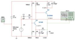
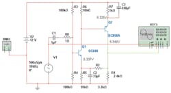
Often, the easiest way to get started is to simply dive in. Accordingly, the feedback amplifier shown in Figure 1 was created as an initial example. A few things immediately became apparent as the parts were assembled. Component and source libraries are listed symbolically on the toolbar. Clicking on a symbol brings up a menu page from which you can drill down further to the required type of part and value.
The components are labeled in the order you enter them although you do have the option to edit the descriptions later. The descriptions are loosely attached to the component symbol so you can move them to a convenient nearby location. There is a difference between editing the label and changing the part’s value. To change the value, you select replace, which brings up a list of available values.
Schematic construction is straightforward and includes an intelligent router. When the mouse cursor hovers over a component, the shape of the cursor changes to become a wiring tool. As you drag and click to make connections, the wiring automatically reconfigures to avoid other wires as well as components. A small dot signifies a connection between wires.
You need to select the type of analysis you want to run as well as the variables to monitor. Here I found the net identification to be awkward. Circuit nets are assigned voltage labels such as V(6), but you have no idea what that refers to. The key is to use the Netlist Report that lists components according to the net number to which they are connected. It’s important to realize that the source V1 is not the same as the net V(1).
Currents are easier to understand because they are directly referenced to a component such as I(R4). To further identify voltages and currents, it’s possible to change the color of the relevant circuit wiring to highlight the measurement made on that net.
I first used the DC analysis feature to make sure the bias levels were about right. It was interesting to watch the convergence process as it iterated the feedback loop performance. Once the component values set the operating points where I thought they should be, I added bypass capacitors across the emitter degeneration resistors to boost the AC gain. I found the multimeter a big help in establishing the correct bias points although the oscilloscopes weren’t quite as easy to use.
I started with the generic version, but neither it nor the Agilent or Tektronix scopes appeared to handle frequencies beyond a few tens of megahertz. It’s only a simulation, so you wouldn’t think that the actual frequency value would make a difference. It probably didn’t, but to get around the problem and gain more experience with AC analysis, I scaled the bypass capacitors to peak the gain around 20 kHz, which seemed to suit the scopes very well.
AC analysis is done with DC sources shorted but with active device model parameters corresponding to the DC operating points. When you use a scope and simply run the simulation, the scope measures the actual DC + AC signal as a real scope would do. Signal clipping is correctly shown.
It’s convenient to be able to add expressions as well as basic voltages and currents to the list of simulated quantities. For example, you can directly evaluate the circuit’s voltage gain and input impedance. Plots can be scaled linearly, logarithmically, in octaves, or in decibels.
For the feedback amplifier, the overall voltage gain is very close to 3,000 and peaks at near 23 kHz as shown in Figure 2a. Because there is a large change in gain with frequency, a logarithmic Y axis is a good choice for the amplitude graph—a familiar log amplitude-log frequency presentation. However, a linear Y scale sometimes shows things that may be confusing on a log scale, especially when very large and very small values are being plotted together on the same graph. A dB plot would have shown that both the input impedance and gain magnitude roll off with frequency at a -6 dB/octave rate, something not apparent from the linear plot.
Changing the scaling from log to linear can be done after the simulation has been run, but in this case, the autoscaling wasn’t done correctly. If the overall plot range was manually constrained to between 0 and 3,000, the plot was correct. When it was allowed to autoscale, the values were 500 too large compared with the actual data values read from a user-positioned cursor or from data exported to Excel. The problem appears to occur when negative logs are needed to scale very small quantities.
A history of the simulation results is available so that you can compare the current performance to previous circuit versions. I found this particularly useful as I varied the amplifier’s frequency response by trying different values for C2 and C3.
Depending on the component values I tried, some of the phase plots exceeded ±Π, resulting in a jump being displayed from +Π to -Π or vice versa. The phase presentation would be easier to understand if it were unwrapped; that is, if it had a continuously increasing or decreasing characteristic. Figure 2b shows the phase plot as Multisim derived it, subsequently exported to Excel.
Discontinuities are common problems in phase plots because the tangent function goes to infinity at ±Π/2. Unfortunately, most implementations of the arctan function are defined only from -Π/2 to +Π/2 so the phase angle is shown with discontinuous jumps each time the arctan function encounters ± infinity. Unwrapping considers the sign of the imaginary and real parts of the transfer function to determine the appropriate quadrant and then modifies the arctan result as required to maintain phase continuity.
As Figures 2a and 2b show, the input impedance phase and magnitude are affected by the shape of the gain amplitude curve, which is related to the amount of feedback available. The further changes beyond 10 MHz are caused by the transistor Ft.
A few simple checks confirm that the general shapes of the curves and their values are correct. The input impedance can’t be greater than 50 kΩ, the parallel resistance of the two bias resistors. Because the voltage gain characteristic initially rises with frequency, it makes sense that the phase should be decreasing from a leading 90°. At the peak of the gain, phase is zero. As the gain falls, the phase approaches -90°, which corresponds to both the rising and falling slopes being at 20-dB/decade, the rate associated with a single zero/pole.
Multisim is a great help when designing a circuit that has several interacting elements. While C2 is decreasing in impedance as frequency increases, the first stage gain is increasing as is the load on the feedback network.
At the same time, because the Q1 and Q2 emitter network time constants are equal, the gain of the second stage is increasing. But as its input impedance decreases, so too does the load on the first stage collector. A feedback circuit such as this one really needs to be designed by separating the forward and feedback networks so the effect of each can be better understood.
Hands-On Digital
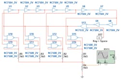
Rather than distinguish between analog and digital, it would have been more accurate to name one section Hands-On Mixed-Signal with both examples under that heading. Multisim uses SPICE models for everything, digital and analog, so you can mix components as required. I chose to design a high-speed stair-step generator based on a ring oscillator as shown in Figure 3. As in the feedback amplifier example, you simply add components from the appropriate libraries and connect them with the wiring tool.
A ring oscillator obviously oscillates, but it can be considered more a case of continuous propagation. There is a metastable condition where all the gates are at an indeterminate voltage between the upper and lower thresholds. In a real ring oscillator, the odd number of inversions guarantees that once an edge starts to propagate through the ring, it will continue. In a simulation, the starting conditions will determine whether an edge ever occurs or the ring just sits there in the metastable state.
Interestingly, Multisim’s transient analysis always showed the ring oscillating. I used Tiny Logic gates in the example, and they have a nominal 100-ns delay. With 10 stages, the ring runs at 1 MHz. There are only nine inversions, but the tenth stage is an OR gate that allows a switch to interactively insert an edge to get things going. This is necessary when running the simulation with a scope, for example.
For both simulation and transient analysis, I needed to reduce the time step to 10 ns from the default 10 µs. Other logic families have different propagation delays so a TTL-based ring no doubt would run faster.
The R-S latches were added to develop drive signals to the resistive DAC that eventually generates the stair-step waveform. Because Multisim is so easy to use, you’re not reluctant to examine circuit operation in more detail than you might otherwise. In this case, probing the outputs of the latches helped me to remember why edge-clocked logic is favored by designers.
In an R-S latch, the two outputs are not complements of each other—you cannot label them Q and Q-bar as you would an edge-clocked latch or flip-flop. They become complementary only as the widths of the R and S signals approach zero. Otherwise, the states of the R and S inputs continue to affect the outputs.
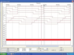
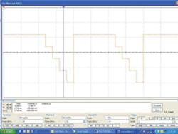
Figure 4 is a screen dump from the logic analyzer virtual instrument display and shows a timing diagram for the four R-S latches. The upper four traces represent the drives to R1, R2, R3, and R5 in that order. The next four traces are the other outputs from the four latches. In each case, the two outputs from each latch are not complementary because of the way in which the R and S inputs are driven.
Because the design included a 1-MHz ring oscillator, I had to use the logic analyzer’s internal clock set to 100 MHz to capture the latch signals. Synchronous capture with an external clock would have been preferred, but the circuit only has several different clock phases. It doesn’t have a suitable high-speed clock that the phases are derived from.
The DAC formed by the resistor network is unique in requiring only one value of resistance. This is important because even simple R-2R DAC structures suffer from scaling and matching problems. In the present case, the only requirement is that all the resistors have the same value. It works as shown in Figure 5—a screen dump from a virtual scope—because of the timing of the R-S latch drive signals.
From Figure 4 it’s clear that the low-going drive signals overlap in time. This means that one, two, three, or all four outputs may be low at the same time and that when one is high, three are low; when two are high, two are low, and so on. The output values are shown in Figure 6 assuming a 2-V Tiny Logic supply. In general, for a circuit with N + 1 resistors, where N – k connect to + V and k + 1 connect to 0V, the output is:
This type of DAC philosophy is similar to the thinking behind a flash ADC that uses a separate comparator for each voltage level being converted. In this R-R DAC, a separate resistor is needed for each output level. Nevertheless, because devices on the same chip can be extremely well matched, this type of DAC is practical and has advantages in some situations.
Summary
I thoroughly enjoyed working with Multisim during this evaluation. The demo version was simple to download and install, and the program worked well. As is the case with most modern applications, many more capabilities are included than you may ever use. By trying both an analog and a digital example, I was forced to consider more simulation and analysis aspects than if I had attempted only one type of circuit.
About the Author
Voice Your Opinion!
To join the conversation, and become an exclusive member of Electronic Design, create an account today!

Leaders relevant to this article:
