Applying Active Load-Pull in Doherty Power Amplifers
In general terms, power amplifiers (PAs) used in communications systems must be large enough to amplify envelope peaks. This leads to amplifiers designed to offer the best efficiency at peak power while actually spending most of the time operating inefficiently, amplifying smaller signals. With the advancement in next-generation communications systems that use signals with ever-increasing peak-to-average ratios, the pressures on the PA design continue to grow.
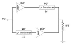
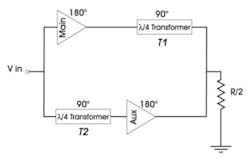
Figure 1. Schematic of a Doherty PA
Techniques such as Doherty amplifier structures extend high-efficiency device operation to lower power levels, allowing for significantly improved average PA efficiency.1 Using active load-pull with waveform measurements can aid in the design and optimization of Doherty PAs. Unlike passive systems, active load-pull systems make it possible to overcome loss and reach all parts of the Smith chart.
The classical Doherty architecture illustrated in Figure 1 consists of Main and Auxiliary devices connected to a shared load via an impedance inverting ?/4 transformer. This transformer, possessing a characteristic impedance equal to the optimum impedance R, allows the impedance of R/2 that exists at the output of the Auxiliary device to be transformed to 2 R at the output of the Main device until the Auxiliary device starts to conduct.
Once the Auxiliary device begins to conduct, the structure itself uses active load-pull between the Main and Auxiliary device, which causes the impedance presented to both devices to vary quite dramatically as a function of the envelope magnitude. The goal is to maintain the high-voltage swing around the Main device, which then allows the high-efficiency operation at peak power to be maintained as the amplifier is backed off. This can be achieved by operating the Main device into higher impedance 2R (twice the optimum at peak power) when the signal level is at its average power level. Then the impedance is reduced to the optimum impedance R as the power increases toward the peak power of the signal. This is achieved using active load-pull from the Auxiliary device.
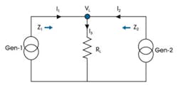
Figure 2. Principle of the Doherty PA Operation
The principle of the Doherty PA operation can be described using ideal current generators as represented in Figure 2. Phase coherent currents I1 and I2 flow within the load, developing the load voltage VL. By pulling the load, the approach allows the possibility of maintaining a constant voltage across the load and, in this case, at the output of Gen-1.
In a Doherty amplifier, the Main device typically is biased in class B, with the Auxiliary device biased deeper in class C. This way, at low power levels up to the average signal power, only the Main device conducts. In this case, the Main device sees only the physical load resistance that has a value of 2R.
When the power becomes large enough for the Auxiliary device to conduct, the current supplied by the device appears as voltage injection at the Main device. As this voltage increases, it gradually reduces the impedance seen by the Main device, reaching the optimum impedance R at the peak power.
At the same time, the impedance seen by the Auxiliary device decreases from a very high impedance as it begins to conduct down to a value of R. So at peak power, both devices are operating into their optimum impedance, both delivering half of the total power. Careful selection of the bias and impedance transforming circuit allows for improved average efficiency of the amplifier.
The classical Doherty structure is closed, RFIN to RFOUT. The RF power division and bias are set within the structure and typically remain fixed. As such, the Doherty design is treated like a black box when measured, characterized, and optimized. This often leads to a design purely conducted in an EDA environment using models that always use some form of approximation for both active and passive circuit elements. As probing the voltage and current directly within the structure is not possible, the structure provides a complex, dynamic impedance environment that can be difficult to understand, sometimes requiring multiple design iterations to meet a desired specification.
To avoid the limitations inherent to a black-box design approach, you must have an in-depth understanding of the behavior of the devices in the amplifier. In this case, a waveform measurement system allows you to vary all of the important parameters that optimize the performance of the Doherty amplifier.
Testing Doherty Structures
The impedance environment within a Doherty structure is complex and dynamic. One way to synthesize it is with an active load-pull measurement system, both in terms of impedance caused by device interaction and the natural impedance caused by the passive structure.
The waveform engineering in the Doherty design synthesizes the complete environment around each device within the Doherty structure. The use of waveform engineering techniques relies on the capability to de-embed back to the current generator plane.
Some software tools allow you to view measurement data at the current generator plane and load-pull the device from this reference plane, making characterization simpler. A waveform engineering approach like this should include synthesis of the input drive, output load impedance, and the bias conditions used while carefully observing the resulting voltages and currents generated.
Measurements begin with the Main device. The object of this investigation is to dynamically vary the load as a function of the input drive. The goal is to maintain a constant voltage swing to maximize efficiency while allowing linear current growth to maintain device linearity.
The first step is to define the appropriate bias condition for the device. The test setup includes a signal source, receiver, and an RF test set connected to the Main device.
The desired class B bias point can be estimated through DC measurements, then confirmed through the generated RF waveforms. A device operating in class B will have well-defined output waveforms, a sinusoidal voltage, and out-of-phase half-rectified current waveform with a 50% conduction angle. The de-embedded current waveforms of an optimized 0.25-W metal semiconductor field-effect transistor (MESFET) device are shown in Figure 3.
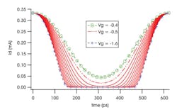
Figure 3. De-Embedded Current Waveforms of a 0.25-W MESFET Device With the Chosen Bias Point Highlighted With a Dashed Blue Line
Now starting at the peak envelope power, the load-pull measurements can be performed to calculate the optimum impedance R. The next step is to store the voltage and current waveforms and reduce the input drive in steps down to the value of the average signal power level as the power is reduced. Waveform engineering then strives to maintain a constant voltage waveform.
Once complete, it is possible to emulate the performance of the Doherty amplifier. For example, using this approach, you can plot the emulated efficiency plateau. In addition, by plotting the waveforms as dynamic load-lines on the I-V plane along with the DC measurement data, it is possible to observe key performance-related behavior, including the proximity of the load-line to the knee-region boundary, as well as any evidence of RF-DC dispersion.
This can be illustrated by analyzing the MESFET device to ensure that the dynamic load-lines are where they should be in relation to the IV plane. There also must be good agreement between the boundary conditions revealed by the dynamic RF load-lines and those defined by the measured DC characteristics.
In addition to this fundamental analysis, the use of active load-pull offers additional benefits to the designer in the form of impedance control at the harmonics. This enables harmonic impedances to be used to engineer the waveforms for optimum performance. Through this approach, it is possible to combine the high-efficiency performance obtained by harmonically optimized amplifiers such as class F and class J realizations with the efficiency plateau that can be obtained from a Doherty design.
Next, we can analyze the Auxiliary device in isolation. Again, the first step is to optimize the bias conditions. In this case, we are trying to bias the Auxiliary device so it begins to conduct as the input power to the Doherty structure reaches the average power of the modulated signal. DC and RF measurements are conducted to do this.
Using the information from the Main device, it then is possible to emulate the impedance environment around this device. This time, the generated voltage also is of interest.
Often, the Auxiliary device causes reliability problems in Doherty amplifiers because it has a very dramatic impedance variation as the power increases. At switch-on, the Auxiliary device sees very high impedance approaching an open circuit, which reduces down to the optimum impedance R at peak power.
It is possible to emulate this using the active load-pull system. Unlike passive systems, it can overcome loss and reach all parts of the Smith chart.
When the device is operating into the high-impedance state, the generated voltage will be large. Analysis of the measured voltage waveforms can show if we are getting close to the voltage breakdown of the Auxiliary device, which could lead to damage, stress, and ultimately failure of the device. To avoid this, the design can be modified. This often is simply a case of altering the gate voltage so the device turns on slightly later, reducing the impedance seen on turn-on.
Finally, with the output matching network in place, measurement system setup can be modified to have dual independent drives. In this case, the measurement system captures only the output performance for this 50-? measurement.
This measurement setup then can be used to consider what happens if there is imperfect phase balance between the Main and Auxiliary devices. This can be used in two ways:
- To consider what would happen if the design did not offer an ideal phase relationship for the Main and Auxiliary devices. This could be particularly useful if the designer were trying to design a wider-band Doherty amplifier where it would only be possible to design the correct relationship at a single frequency with trade-offs used to design the relationship over the rest of the band.
- To allow you to correct for AM/PM behavior before the design is manufactured.
Once the investigations are complete, the design can be finished by attempting to realize a matching network to recreate the optimum conditions discovered using the measurement system. Inevitably, there will be some design trade-offs which means that compromises will be necessary.
Accordingly, once the passive circuit environment has been designed, it often is useful to repeat some of the measurements using the waveform measurement system to give a more realistic idea of the performance that can be expected from the manufactured design. If the desired specifications are not met, additional optimization of the design can be conducted, each time using the measurement system to verify the performance. By the time the design is committed to manufacture, there is greater confidence that the design will meet the specifications.
Other Doherty Structures
Designing with immature device processes and materials can add difficulties to PA design. Here the capability to observe the dynamic load-line behavior through the measurement of voltage and current waveforms can be invaluable.
Using the waveforms to compare the dynamic RF performance at the de-embedded current plane with the DC performance can give you a clear understanding of device-related issues. It also can offer insight into bypassing the problem through appropriate redesign, such as operating the device under different bias/load conditions.2,3
Example measurements are described using a GaN transistor. These measurements were conducted when GaN was still an immature process, but it could easily be applied in a similar way to transistors based on new materials such as diamond.
Figure 4 shows the waveforms obtained for the Main device from a GaN Doherty structure biased at a drain voltage of 17 V. As expected, the voltage magnitude remains relatively constant, and the magnitude of the half-wave rectified current waveform grows with increasing input drive. On closer inspection, there is some current compression evident at higher drive levels, and the maximum magnitude of both voltage and current are lower than expected. This is more noticeable when the waveforms are viewed as dynamic load-lines.
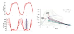
Figure 4. Waveforms Obtained for the Main Device From a GaN Doherty Structure
The dynamic load-lines collected at different load and drive conditions map out a separate RF knee region. This device had two well-understood problems often seen with early GaN devices: current slump and knee walkout. Such problems become progressively worse for increasing drain voltage.
The initial measurements yielded a plateau of relatively low efficiency between 30% and 40% over an 8-dB dynamic range together with a maximum output power of 28 dBm, almost 3 dB lower than initial designs suggested was possible.
The analysis shows how the device’s knee voltage has crept from 3 V to 6 V and how the available RF current has collapsed from approximately 500 mA to 300 mA. Compounding these problems, the resulting suboptimal impedance presented to the device results in disappointing output power and efficiency.
To re-optimize the Doherty structure so the effects of knee voltage walkout are reduced, more large-signal measurements were conducted using a drain voltage of Vd = 12 V. This allowed for a reduced slumped current of 350 mA and the reduced knee voltage of 3 V. Using this approach, the value of R was conveniently maintained at 50 ?, allowing the same structure to be used.
A new dynamic load-line in Figure 5 shows that the collapse in knee voltage is not as significant and has receded to somewhere in the region of 3 V for a similar maximum current of 300 mA. When device performance is reconsidered in comparison to the Vd = 17 V case, testing reveals a plateau of improved efficiency between 40% and 50% over an 8-dB dynamic range, representing an approximate 10% improvement. This is alongside a maximum output power of 27.5 dBm, only marginally lower than the Vd = 17 V case.
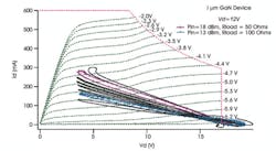
Figure 5. A New Dynamic Load-Line Showing Improved Efficiency
Conclusion
An active load-pull system can be used to design and, perhaps more importantly, optimize Doherty designs. The approach can independently measure and optimize the Main and Auxiliary devices. Then, the output stage design can be completed and the system reconfigured to look at the input of the structure. This is particularly useful for a wide-band Doherty design where the effects of uneven phase of the drive signal can be observed.
Using this information, it also may be possible to take account of AM/PM behavior and compensate with the input architecture. A case also was examined where an immature device technology—an early immature GaN transistor—was used for the Doherty design. The current and voltage waveforms, plotted as a dynamic load-line, were used to diagnose a device-related problem and allowed re-optimization of the design before manufacture.
More importantly, the measurement system also allows optimization of harmonic impedance, enabling the designer to improve overall efficiency performance by combining the Doherty amplifier approach with a harmonically tuned class of operation.
By capturing the right set of measurements and then re-optimizing the design before manufacture, the design cycle can be significantly decreased, reducing time to market for new products. In addition, by considering time-domain waveforms within the design process and through appropriate design techniques, the reliability of the Doherty amplifier also can be improved.
References
1. Doherty, W.H., “A New High-Efficiency Power Amplifier for Modulated Waves,” Proceedings of the Institute of Radio Engineers, May 1936.
2. Lees, J., Benedikt, J., Hilton, K.P., Powell, J., Balmer, R.S., Uren, M.J., Martin, T., and Tasker, P.J., “An Experimental Gallium Nitride Microwave Doherty Amplifier,” Electronics Letters, Institution of Engineering and Technology, November 2005.
3. Lees, J., “Doherty Amplifier Structures for Modern Microwave Communication Systems,” Ph.D. Thesis, Cardiff University, 2006.
About the Authors
Darren McCarthy is the RF technical marketing manager at Tektronix. He has worked extensively in various test and measurement positions for more than 25 years, including R&D engineer and project manager, product planning, and business and market development. During his career, Mr. McCarthy has represented the United States and Tektronix as a technical advisor and working group member on several industry standard groups and forums. He holds a B.S.E.E. from Northwestern University. Tektronix, [email protected]
Tudor Williams, Ph.D., is the senior systems engineer at Mesuro. He received a master’s of engineering in electronic and communications engineering from Swansea University and a doctorate from Cardiff University. Dr. Williams later worked as a research associate at Cardiff University, and from there he was with Selex Galileo where he designed ultra-wideband x-Band MMICs for military applications. Mesuro, [email protected]
About the Author
Comment About the Article
To join the conversation, and become an exclusive member of Electronic Design, create an account today!

Leaders relevant to this article: