Keeping Up With PCIe 3.0 Test Requirements Part 1

With the release of new and improved specifications for SATA, USB, and now PCI Express (PCIe), the era of third-generation (Gen3) serial data has arrived. Not only are the new specifications faster, they also push the limits of what is possible within the constraint of backward compatibility and high-volume manufacturing materials and tolerances such as FR4 boards, connectors, and backplanes.
With each of the Gen 3 standards comes new design and test challenges, and PCIe 3.0 is no exception. While test complexity always increases with each generation, Gen 3 serial standards are changing the game with more involved compliance tests, new equalization schemes, de-embedding, and required receiver characterization tests. Troubleshooting and debugging also are more demanding with higher speeds leading to greater sensitivity to jitter and other noise.
PCIe 3.0 Overview
PCIe 3.0 is the next evolution of the ubiquitous and general-purpose PCIe I/O standard. At an 8-GT/s transfer rate, the interconnect performance bandwidth is doubled over PCIe 2.0 while preserving compatibility with software and mechanical interfaces. The PCI-SIG released the final PCIe 3.0 specification on Nov. 17, 2010.
Motherboards and graphic cards with a modest level of PCIe 3.0 support, or at least compatibility, are appearing with higher volume. General adoption is expected toward the end of the year and mainstream adoption further into 2012.
Helping to accelerate adoption will be Intel’s Ivy Bridge chipsets due Q1 2012. This next generation of LGA1155 Processors will feature PCIe 3.0 support to connect with graphics cards.
To say that PCIe is important is something of an understatement. In 2010 alone, analysts estimated that PCIe was used in more than 440 million devices, mostly computers but in many other embedded devices and 37 million communications boards. By offering backward compatibility with previous generations, PCI-SIG has ensured that PCIe 3.0 will maintain this momentum and remain the interconnect of choice across the industry for motherboards, graphics cards, and other peripheral devices.
The PCIe 2.0 bit rate is specified at 5 Gb/s, but with the 20% performance overhead of the 8b/10b encoding scheme, the delivered bandwidth actually is 4 Gb/s. PCIe 3.0 uses a more efficient 128b/130b encoding scheme. By removing this overhead, the interconnect bandwidth doubles to 8 Gb/s with the implementation of the PCIe 3.0 specification. This bandwidth is the same as an interconnect running at 10 GT/s with the 8b/10b encoding overhead. As a result, the PCIe 3.0 specifications deliver the same effective bandwidth but without the penalties associated with 10-GT/s signaling, such as greater PHY design complexity and increased silicon die size and power.
To accommodate the higher speeds, PCIe 3.0 electrical signaling implementations require the use of equalization to open the eye on the receiver (Rx). Equalization is a method of distorting the data signal with a transform representing an approximate inverse of the channel response. It may be applied at the transmitter (Tx), the Rx, or both.
A simple form of equalization is Tx de-emphasis as specified in PCIe 1.x and PCIe 2.x where data is sent at full swing after each polarity transition and at reduced swing for all bits of the same polarity thereafter. De-emphasis reduces the low-frequency energy seen by the Rx. Since channels exhibit greater loss at high frequencies, equalization reduces these effects.
Equalization may be implemented using various types of algorithms; the two most common are linear (LE) and decision feedback (DFE). LE may be implemented at the Tx or the Rx while DFE is implemented at the Rx.
Trainable equalization refers to the capability to adjust the tap coefficients. Each combination of Tx, channel, and Rx has a unique set of coefficients yielding an optimum signal-to-noise ratio. The training sequence consists of adjustments to the tap coefficients while applying a quality metric to minimize the error. The choice for the type of equalization depends largely on the interconnect channel optimizations that can be derived at the lowest cost point.
Measurement Challenges
Since PCIe 3.0 uses the same FR4 circuit board material and connectors as the previous generation but greatly increases data transfer rates, this opens a Pandora’s Box of measurement challenges and potential design issues. For instance, just opening the data eye at the Rx requires new techniques for both Tx and Rx equalization that, in turn, means that channel embedding is necessary for compliance testing. Here are some other considerations:
- PCIe 3.0 base spec measurements are defined at the pins of the Tx. Unfortunately, the Tx pins typically are not accessible, meaning that breakout channels will need to be created and de-embedded to do the measurements.
- Equalization on either the Tx or Rx side only compensates for channel loss or data-dependent jitter (DDJ). New jitter measurements have been defined that account for the separation of DDJ and uncorrelated deterministic jitter.
- Rx testing becomes a requirement to ensure system interoperability. It no longer is sufficient to test only the Tx and expect that two compliant products will work together in a system. Signal integrity variations are such that Rx stress tests become crucial in determining system reliability.
- On PCIe 3.0 protocol verification, link training and power management present difficult protocol-layer test challenges. Tools that help bridge the electrical and protocol layers of the physical layer will be required to debug these issues.
Resolving Test Challenges
Let’s look at electrical testing challenges, beginning with the Tx test step. As with previous versions of PCIe, Tx compliance will be measured using the PCI-SIG’s SigTest utility as a reference. This tool formally was used during PCI-SIG compliance workshops.
For PCIe 3.0, all compliance measurements are defined in the compliance test specification (CTS). The CTS is based on the card electromechanical (CEM) specification. The CTS currently is being defined within the Serial Enabling Group of the PCI-SIG.
PCIe 3.0 requires two tests for the Tx. The first is an electrical test that is similar to PCIe 2.0. Next is a preset test that verifies that the Tx de-emphasis and pre-shoot are within the limits for all Tx equalization settings or presets. All tests are run using the new compliance pattern.
Unlike previous versions of PCIe, all measurements are taken after embedding the compliance channel. There are two compliance channels: one for system and one for add-in card testing. New compliance boards are being developed, but PCIe 3.0 Tx testing can be done on the PCIe 2.0 compliance base and load boards.
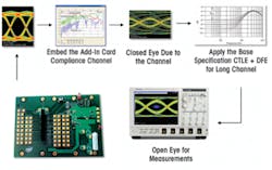
Figure 1. Diagram Showing That Compliance Channel Must Be Embedded Before Taking Measurements
Let’s look at the compliance testing process and the post-processing required to take the measurements using the example of testing an add-in card. The add-in card is inserted into the compliance baseboard, and the signal is directly acquired into the scope.
As shown in Figure 1, the eye is open when it is acquired; however, before taking any measurements, the compliance channel must be embedded. S-parameter files that represent the channel used to embed the channel will be provided by the SIG. Once the channel has been embedded, the eye is closed, and a reference equalizer must be applied to open the eye before the measurements can be taken. The measurement limits are defined within the CEM specification.
For PCIe, there are seven continuous time linear equalization settings. Before the measurements are taken, the optimal Rx equalization is determined for each preset. Once the optimal setting has been determined, the final measurements are taken.
The eye height after Rx equalization can be as small as 34 mV and still pass the compliance test. This has implications on oscilloscope performance. Taking these measurements requires the optimal balance of instrument bandwidth and noise contributed by the test equipment. As bandwidth increases, with any oscilloscope, noise increases.
Part 2
With the added complexity of PCIe 3.0, there is the need for tools that address more than just compliance testing. Part 2 of this article, which will appear in the September issue of EE, will explain the approaches beyond simple SIG tests that can help to implement complex PCIe 3.0 designs. The focus will be on the proper application of new debug and characterization tools, de-embedding, jitter and timing analysis, receiver characterization, and protocol verification.
About the Author
Chris Loberg is a senior technical marketing manager at Tektronix. He has held various positions with Tektronix during his 13 years with the company, including marketing manager for the Optical Business Unit. His background in technology marketing includes working at Grass Valley Group and IBM. Mr. Loberg holds an M.B.A. in marketing from San Jose State University. [email protected]
About the Author
Comment About the Article
To join the conversation, and become an exclusive member of Electronic Design, create an account today!

Leaders relevant to this article: