Keeping Up With PCIe 3.0 Test Requirements Part 2
Part 1 of this article appeared in the August issue of EE.
The era of third-generation (Gen 3) serial data arrived with the release of new and improved specifications for SATA, USB, and PCI Express (PCIe). Not only are the new specifications faster, they also push the limits of what is possible within the constraint of backward compatibility and high-volume manufacturing materials and tolerances.
With each Gen 3 standard comes new design and test challenges, and PCIe 3.0 is no exception. While test complexity always increases with each generation, Gen 3 serial standards are changing the game with more involved compliance tests, new equalization schemes, de-embedding, and required receiver characterization tests. Troubleshooting and debugging also are more demanding with higher speeds leading to greater sensitivity to jitter and other noise.
Beyond SigTest
With the added complexity of PCIe 3.0, there is the need to have debug and characterization tools that go beyond compliance testing. For instance, what happens if the measurement fails SigTest? How will you gain further insight into the failure?
In some cases, the failure could be caused by the channel so you would want to look at the waveform before the channel has been embedded or look at embedding a different channel to see if the results are changed. In addition, you might want to double-check the receiver (Rx) optimization settings that were chosen by SigTest. Other times, you may want to look at the output of the transmitter (Tx) or change measurement parameters to provide deeper analysis.
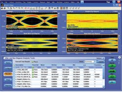
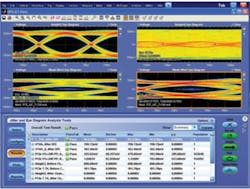
Figure 1. Tools Providing Visibility Into the Signal at Each Stage of the Transformation Process
We have determined that a -8 dB continuous time linear equalization (CTLE) function is the optimal for a system, and now we are ready to do the card electromechanical (CEM) measurements. The increase of post-processing techniques to condition the waveform before analysis makes it difficult to know how the waveform has been transformed before the final measurements are being processed. In addition to providing pass/fail results as per the specification, more advanced tools can provide full visibility of the signal at each stage in the transformation process.
In Figure 1, the signal as it has been acquired in the eye diagram appears on the top left side. The compliance channel is added to the waveform as shown in the top right side. The bottom left shows the waveform after the CTLE has been applied. Even without the application of the decision feedback (DFE), the signal has passed Tx requirements. The application of the DFE opens the eye further.
However, if a failure occurred after the application of the DFE, the engineer has the insight to go back and ensure that the optimal CTLE has been applied. In this case, if a -12 dB CTLE setting had been selected, the test would have failed.
Debug and Characterization Tools
Since capturing a signal through cables and fixtures distorts the signal shape, PCIe 3.0 compliance and debug testing require the need for a fixture de-embedding capability to remove the effects of the fixture from the measurement. Fixture de-embedding and the resulting improved accuracy of your measurement might make the difference between pass and fail of the test. De-embed filters typically are created using link analysis software and then saved as the base specification for measurement setup for future use.
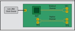
Figure 2. A PCIe 3.0 Test Board
Figure 2 is a simplification of actual test boards that may include multilanes and breakout channels to match the different run lengths of each lane’s breakout channel. The idea is to obtain the S-parameters of the replica channel to create a filter to de-embed the effects of the channel. Typically, this is done using the TDR functionality of a sampling oscilloscope and link analysis software to create the de-embed filter. The signal then is acquired after it has gone through the breakout channel with the goal of replicating the signal as it occurred at the pin of the Tx.
Another challenge results from the Tx signal shape. The signal no longer is a simple non-return-to-zero (NRZ) square wave pattern. PCIe designers alleviate high-frequency loss in the media with Tx equalization with pre-emphasis or de-emphasis of the Tx waveform. Since Tx signals need to be evaluated for this Tx equalization, test tools should provide complete Tx equalization insertion or removal.
An important part of PCIe 3.0 links will be evaluation of the complicated interaction between the measured waveform and the lossy behavior of the interconnect channel. It no longer is possible to assume that if the Tx output meets the eye diagram mask, a design will work against all channels up to a given loss. Instead, advanced serial data link analysis methods are needed to acquire the true Tx waveform and then test against several stressed or lossy channel situations.
In some cases, this test can be performed with real physical channels: Connect the Tx under test to the suite of normative test channels, one channel at a time, and for every channel, evaluate the signal shape at the Rx end. Oscilloscope measurement systems and jitter and eye analysis software will provide a complete measurement facility for accurate measurements of the resulting waveform.
However, this methodology still is prone to errors. Are the physical normative channels really normative? Certainly, each physical device has tolerances against the standard’s ideal values. Furthermore, the physical channel can be difficult to reconstruct in a silicon design lab if representative materials do not exist for reliable channel recreation. In this case, a virtual channel would be more convenient to use in performing link analysis.
Since physical corner-case channels typically are not conveniently available, the Tx test that includes corner-case channels uses virtual channels based on the network description file, in particular on S-parameter touchstone files. Such description of compliance channels is part of the PCIe 3.0 test specification.
In this case, the measurement on the Tx under test simply involves acquisition of the Tx signal. Then the captured signal is connected to all desired test channels, one channel at a time—in software emulation rather than physically. When this methodology is supported, the interaction of test channels with the Tx can be viewed without the need to reacquire the Tx waveform.
Jitter and Timing Analysis
The increased speeds of PCIe 3.0 mean reduced circuit tolerance or margin for jitter and related signal integrity problems. By using tools that can help to characterize and discover sources of jitter and signal integrity concerns, engineers will be able to bring products to market that deliver the expected performance with more confidence that they will operate reliably.
Analysis plots like spectrum and trend go beyond simple measurements and results display. Trend analysis indicates how timing parameters change over time, like frequency drift, phase-locked loop (PLL) startup transients, or a circuit’s response to power supply changes. Spectrum analysis quickly shows the precise frequency and amplitude of jitter and modulation sources for easy, rapid identification. Finding jitter sources like adjacent oscillators and clocks, power supply noise, or signal crosstalk is critical to bringing designs to market quickly.
Phase noise plots are useful for showing jitter in root/Hertz and transfer function plots that allow direct comparison of jitter spectrums between two signals of differing frequencies. They provide a way for determining jitter in PLL circuits like clock multipliers.
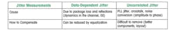
Table 1. Importance of Separating Data-Dependent Jitter and Uncorrelated Jitter
With PCIe 3.0 come new jitter measurements that have separate limits for data-dependent jitter (DDJ) and uncorrelated deterministic jitter (UDJDD). With the data rate increase from 5 GT/s to 8 GT/s and the more advanced methods of compensating for channel loss, it is important to separate DDJ, which can be compensated with Tx and Rx equalization, and UDJDD, which can be caused by effects such as crosstalk and power supply noise as detailed in Table 1.
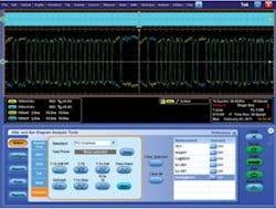
Figure 3. Test Tools for PCIe Jitter Measurement
Similar to PCIe 2.0, tools are becoming available that provide the complete set of PCIe 3.0 jitter measurements as shown in Figure 3. These tools enable designers to verify that their silicon meets the base specification requirements.
Pulse width jitter (PWJ) is an important measurement that addresses the increased channel loss at 8 Gb/s. The purpose of the PWJ measurement is to ensure that lone bits meet minimum pulse width requirements. A new jitter measurement that will be supported is Q-scale extrapolation as defined in the base specification.
In addition to jitter, other PCIe 3.0 base specification measurements are voltage, package loss, and Tx equalization. The voltage measurements include the addition of the Tx-EIEOS measurement. This measurement is required to ensure that a receiver can properly detect the exit from electrical idle.
The package loss measurement ps21 captures the silicon package loss and drive characteristics. The Tx equalization measurement verifies that the pre-shoot and de-emphasis for each preset meet the requirements of the specification.
Bandwidth Considerations for Tx Testing
As in any Gen 3 test environment where signal integrity is critical to margin test evaluation, it is important to balance instrument bandwidth with application requirements. For instance, instrument-based inherent noise has the tendency to increase with bandwidth, which may reduce accuracy and measurement margins. However, it also is important to have sufficient bandwidth to capture the high-frequency content of the signal.
There are other considerations as well. If it is possible to probe near the Tx pins, then a higher bandwidth scope is preferred. Also for debug, there may be signal transients such as reflections or crosstalk that can be filtered by a lower bandwidth instrument. In situations like this, a 16-GHz oscilloscope or higher will produce the best results.
For applications that involve de-embedding noise, amplification is a primary consideration because de-embedding involves boosting the higher frequencies to compensate for the frequency-dependent losses. Compliance testing is performed at the end of a channel, and consequently, harmonic content of the signal has been lost, and the rise time of the signal has been slowed due to channel loss. In most cases, a 16-GHz oscilloscope provides the most flexibility to support different PCIe 3.0 test conditions that involve de-embedding.
Conclusion
With the release of the PCIe 3.0 specification in 2010, the era of 3.0 actually has arrived. The big adoption curve will start later in 2011 as electronics manufacturers begin introducing fast motherboards and video cards to take advantage of the 8-GT/s performance.
However, in an effort to manage costs and ensure backward compatibility, PCIe 3.0 will continue to utilize the same FR4 circuit board technology as its primary electrical signaling path. Using this 10-plus-year-old technology for 8 GT/s signaling creates many new challenges for predictable performance from a signal integrity perspective.
As demonstrated through an illustration of new Tx testing approaches, successful implementation of PCIe 3.0 designs will require that engineers go beyond simple SIG tests. Knowledge of and proper application of new debug and analysis tools for Tx testing, de-embedding, Rx characterization, and protocol verification will lead to successful implementation of this new technology in the computer market segment.
About the Author
Chris Loberg is a senior technical marketing manager at Tektronix. He has held various positions with Tektronix during his 13 years with the company, including marketing manager for the Optical Business Unit. His background in technology marketing includes working at Grass Valley Group and IBM. Mr. Loberg holds an M.B.A. in marketing from San Jose State University. [email protected]
About the Author
Comment About the Article
To join the conversation, and become an exclusive member of Electronic Design, create an account today!

Leaders relevant to this article: