Applications such as those involving electromobility require high-quality miniaturized power electronics to complement electric and hybrid drives.
The manufacture of such power electronic devices in production volumes and at high yields imposes significant new challenges, including the development of test methods that efficiently guarantee fault-free devices. One approach includes high-level inspection technologies such as 3-D X-ray analysis to look for solder voids that can degrade device quality.
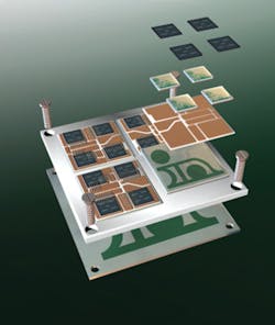
Figure 1. System Layout of an Integrated Power Module
Courtesy of Indium
Required Production Technology
The production of power-electronics devices typically involves direct mounting of dies such as IGBT or diodes on a basis substrate. Large soldering areas on the bottom sides of the dies and parallelized bond connections at the top sides implement the required electric connections.
Often, the basis substrate is soldered on a heat sink to dissipate power. For devices used in power control for hybrid vehicles, the heat sink also is integrated in the vehicle’s cooling-water circuit. Figure 1 shows the schematic system layout of an integrated power module.
Open Doors for Excess Heat
Maximum heat transfer must be guaranteed from the soldered die to the heat sink to ensure the power modules are reliable and durable. Low thermal resistivity can achieve the required thermal coupling, but voids within solder connections play a decisive role in degrading this coupling. Especially in large-scale solder joints that may cover an area of up to 25 cm², avoiding the development of enclosed gases is difficult. Often, voids of different sizes and positions remain within this connection. In terms of thermal coupling, they may lead to the module’s malfunction or even destruction in the operation mode.
Making the Invisible Visible
The current state of technology offers few opportunities to detect voids after the soldering process. A 100% test within the production cycle even limits the selection of test technologies. Acoustic microscopy and computer tomography by means of an X-ray analysis system are not efficient because of the time scales required for image capturing and evaluation.
In principle, the X-ray technology is effective for solder-joint analysis on electronic assemblies and widely used for quality control in the inline production process. However, for power devices, this inspection technology faces new challenges:
- Safe and high-resolution detection of voids in relevant solder joints
- Separation of voids in various layers
- Determination of quality affecting parameters for each solder layer (void, sum of all voids, local distribution of voids)
- Inspection in mounted state (for example, with heat sink)
- 100% inspection in the production cycle
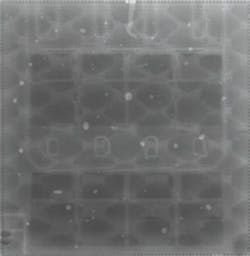
Figure 2. X-Ray Image of an Orthogonally or Angularly Radiated PCB
Common 2-D and 2.5-D X-ray inspection systems are unsuitable for such tests. A view of an orthogonally or angularly radiated PCB illustrates the problems (Figure 2). Voids are visible but cannot be referenced to a specific solder layer. However, this classification is very important because significantly different quality criteria are set for the thermal coupling of die and basis material as well as basis material and heat sink. Consequently, an evaluation of voids detected with a 2-D or 2.5-D method would lead to fault escapes or massively increased false rejects of the device.
Skillful Inspection Bit by Bit
The only remaining method for quality assurance is 3-D X-ray inspection technology that can completely reconstruct layers. This methodology also faces particular challenges, and not every system is able to handle this sophisticated test task.
A critical reason is the already mounted heat sink that features structures for a possibly large contact surface with the cooling medium, especially for the integration in a cooling-water circuit. These structures cause different X-ray absorptions to appear as faults in the reconstructed result image. Similarly, solder-joint sizes as well as the undefined position and dimension of voids affect such artefacts when utilizing standard reconstruction methods. As a result, a 3-D X-ray inspection system has been enhanced to capture the adapted image and enable layer reconstruction.
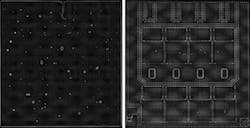
Figure 3. Layers Between Die Basis Material and Basis Material Heat Sink Separated With Adapted Reconstruction Method
The captured images in Figure 3 facilitate automatic void detection in each layer including classification in terms of quality parameters determined separately for the respective layers. Furthermore, there is the opportunity to survey and evaluate faults at a verification station.
The automated X-ray inspection system also is suitable for the inline inspection of double-sided PCBs. In just one run, all PCB layer information is available and can be individually reconstructed for automatic analyses. This characteristic provides the opportunity to break down critical solder joints, such as under BGAs, into single layers for detailed automatic analysis. For this reason, complete 3-D X-ray inspection in the production cycle provides the basis for comprehensive quality analysis and the highest production quality.
About the Author
Jens Kokott has been working for GÖPEL electronic GmbH in Jena, Germany, as senior manager of automated inspection since 1992. Previously, the graduate engineer studied instrument and precision engineering and business studies at the Friedrich-Schiller-University in Jena and the Open University Hagen/Germany, respectively. From 1991 to 1992, Mr. Kokott was an assistant lecturer at the Jena university.
GOEPEL electronics, 9737 Great Hills Trail, Ste. 170, Austin, TX 78759, 512-782-2500, www.goepelusa.com


