In-circuit test (ICT) has been instrumental in identifying manufacturing process defects and component defects on countless varieties of populated printed circuit board (PCB) assemblies for more than 40 years. ICT operates by gaining direct electrical access to the board under test through a bed-of-nails fixture and other limited-access techniques including IEEE 1149.1 boundary-scan and IEEE 1149.8.1 powered opens. When performing electrical tests, each active and passive component typically is isolated from other surrounding components and tested on an individual basis.
Passive components including resistors, capacitors, inductors, and circuit-protection devices compose the highest percentage of all devices that are populated on today’s PCB assemblies. However, the successful isolation and testing of these components during ICT is perhaps the most challenging and the least understood of all modern-day validation practices.
Measurement Basics
There are two common methods used to measure the resistance, inductance, and capacitance (RLC) of a device. The first is to force an AC current and measure the AC voltage drop across the component. A second method is to force an AC voltage across the component and measure the resultant AC current flowing through the impedance.
Any surrounding components electrically connected to the DUT are neutralized from affecting the measurement by a process known as guarding, which can be either passive or active in nature. In addition, the AC stimulus voltage typically is made low enough in amplitude to avoid accidentally turning on integrated circuit P-N junctions that may be attached to the DUT.1
The voltage and current measurement data typically is created from a discrete time digitization of the two continuous time waveforms in a phase coherent manner. This results in two data vectors that then are numerically operated upon to extract the impedance value.
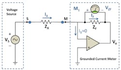
The preferred ICT metrology, shown in Figure 1, uses a voltage source as a stimulus generator (VS) and a transimpedance amplifier or a virtual ground current meter to detect the current (IX) that flows through the unknown device (ZX). The source voltage and device current are both complex numerical values denoted in either Cartesian form (V = A + jB) or in polar form (V = |V| ejθ).
The calculated component impedance is the quotient of the complex voltage impressed across the device divided by the complex device current. Impedance is a complex value that changes as a function of the applied test frequency.
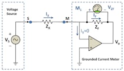
Again, referring to Figure 1, if the op-amp has negligible bias current (IB 0) into the negative input terminal, then all of the current flowing through the unknown impedance (IX) also will flow through the op-amp feedback impedance ZF, making IX equal to IF. Additionally, the op-amp differential input voltage (V+ – V-) is approximately equal to the output voltage VO divided by the op-amp open-loop gain AVO, which typically is a very large number at lower frequencies.
If the op-amp output voltage is limited to ±10 V and AVO = 2 x 10⁶ V/V, then the maximum voltage across (V+ – V-) will be only ±5 µV, thereby making the negative input terminal at a virtual ground potential. Finally, the output voltage VO and the voltage across the feedback impedance can be described as follows:
Knowing the stimulus voltage amplitude VS, the value of ZF and the voltage VZF across ZF allows you to readily calculate the complex value of the unknown component:
where: Vs and θVS = the respective magnitude and phase
angle of the stimulus voltage
VZF and θZF = the respective magnitude and phase angle
of the voltage across the feedback impedance
Calculating the real part of ZX will return the resistive component of the impedance while calculating the imaginary component will yield the inductive or capacitive reactance value. To minimize measurement errors at higher test frequencies, ZF also needs to be treated as a complex number.
If the DUT is purely resistive, then the phase information is not required and Z can be replaced with R. Equation 2 reduces to:
Equation 3 can be used to calculate an unknown resistor value by using a DC source voltage rather than an AC stimulus. However, when using DC rather than AC to measure a resistor value, care must be used to minimize any DC offsets and thermal EMFs from relays and dissimilar metal junctions in the stimulus, measurement, and guard paths because they can have a negative impact on the accuracy of the measurement.
Two- and Three-Terminal Measurements
The circuit configuration in Figure 1 is called a two-terminal or two-wire measurement because only source and measure connections are used. This arrangement rarely occurs on populated PCB assemblies because other components typically are connected to the device being tested. Guarding must be used to eliminate the negative effects of these other components.
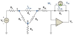
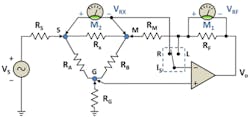
Figure 2 shows a simplified circuit where the DUT (RX) is connected to other components (RA and RB) and indicates how to connect guard terminals to isolate the DUT. For simplicity, these complex impedances now are shown as simple resistances in the figure. Wire terminal resistances RS, RM, and RG also are shown. With no passive guard in place at node G, a current divider would be created between RX and the series combination of RA and RB. As a result, current would flow through both parallel paths and an error in the measurement would occur.
With the passive grounded guard G in place, RA now is shunted across the low output impedance source, and RB is placed across the op-amp V- and V+ input terminals. With virtually no voltage present across the V- to V+ terminals, there is negligible current flow through RB. Virtually all of the current flowing through RX also flows through RF, where the unknown device current is measured with meter M1.
Four- and Six-Terminal Measurements
Path resistances RS, RM, and RG can degrade the accuracy of the measurement and may need to be compensated for with additional measurement terminals. For example, if RA is a low-impedance device, then current will flow through it and through the non-zero parasitic guard resistance RG. This current will create a voltage at node G that ultimately will force a current through node M and introduce an error in the measurement of the DUT current VRF/RF. The wire resistances RS and RM also will affect the measured value of RX. The calculated measurement value of RX that includes the error effects of residuals RS, RM, and RG for Figure 2 is shown in Equation 4:
where: Rxcalc = the calculated resistance value including measurement errors
RS = the source lead resistance
RM = the measurement lead resistance
RX = the resistance being measured
RG = the guard wire resistance
RA = the Thevenin source-side guarded resistance
RB = the Thevenin measurement-side guarded resistance2
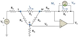
Minimizing the guard error caused by the finite resistance RG can be achieved by allowing the noninverting terminal of the op-amp input to sense the voltage at node G remotely. This configuration, shown in Figure 3, is what is commonly called a four-wire guarded measurement, not to be confused with a four-wire Kelvin measurement. With the addition of this fourth terminal, there typically will be negligible voltage across RB and therefore negligible error current through RM that would be injected into the transimpedance amplifier from node G.
Adding another two terminals or wires can help to eliminate the errors caused by the source and measure wire resistances RS and RM. This six-wire metrology is illustrated in Figure 4. Two possible options to connect the op-amp’s negative input terminal are represented by the single-pole, double-throw switch. In position L, the op-amp current sense terminal is in the local position while the R position denotes a remote sense position. If there is no need for guard terminal(s) or a guard sense terminal, the configuration will reduce to a classic four-wire Kelvin connection scheme that still will help mitigate the source and measure wire losses resulting from RS and RM.
Referring again to Figure 4, the digitizer measurements can be made with two individual meters M1 and M2 that may have individual gain (K1, K2) and offset errors (Voffset1, Voffset2). These gain and offset terms, even if calibrated out, may drift over time and temperature, negatively affecting the measured value of RX (Equation 5).
However, if a single digitizer is used that is multiplexed between measuring the RX voltage and the RF voltage, the gain errors K1 and K2 tend to mathematically cancel because they are nearly the same value. Further, if the real and imaginary terms of the measurement are extracted through a single-bin discrete Fourier transform, then the DC offset terms can be eliminated from the measurement bin. Additionally, the impedance instrument can be designed to interleave alternating measurements of DUT voltage VRX and DUT current VRF/RF within a single or multiple AC cycles, thereby adding no additional test time for the unit test period.
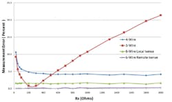
A plot of the percentage error as a function of the value of RX for 3-wire, 4-wire, and 6-wire local and remote current sense measurements is illustrated in Figure 5. The conditions for this plot are RS = RM = 0.8 Ω, RG = 0.4 Ω, and RA = RB = 50 Ω. The error increase of the 3- and 4-wire measurements below about 200 Ω is caused by the series resistances RS and RM while the increase in the 3-wire plot above 200 Ω is a result of the combination of the guard voltage G and a low value of RB that continues to inject error current into the current meter as the current from RX is diminishing with increasing RX values.
The error for the 6-wire local sense metrology is largely caused by the IR drop across RM. This voltage drop becomes impressed across RB, creating an error current through RB as well. The remote sense current meter (switch in the R position) further improves the overall accuracy of the measurements by removing both of these errors. In theory, the 6-wire remote sense configuration removes all errors except for the finite loop gain error and the input offset error associated with the current meter. Not all ICT platforms can realistically support 6-wire configurations because of limited instrument design or sparse multiplexing ratios.
DUT Equivalent Circuits
Most in-circuit testers can return series and parallel equivalent circuits involving CS, CP, LS, LP, RS, and RP for a given impedance measurement. When measuring a capacitor with no physical series or parallel resistors in the circuit, it is sometimes not clear whether CS or CP should be used. The calculated values of CS and CP can be quite different because of the quality of the component, the measurement path resistance, the component value, and the applied test frequency.
As a general rule of thumb, if the capacitor has a value less than 10 nF, CP should be used because the parallel resistance is likely to have a more significant effect on the measurement than the series resistance. Above about 1 to 10 µF, the parallel resistance is likely to have less effect than the series resistance, so CS should be used in these instances. Similarly, low values of resistance generally should use RS while high values should use RP. Comparing the reactance of a capacitor or inductor to the parasitic resistance values can help in determining whether to use a series or a parallel model.
Other Test Considerations
When testing a component, it may not be clear which pin should be the source node and which pin should be the measurement node. The key to determining the best connections for the test is to consider what else is connected to the pins of the DUT. For example, if one lead of the DUT is connected to a super node such as a power or ground node, this lead should be placed on the source side rather than on the current meter’s measurement pin. With a super node, many other nodes will need to be guarded and that will place a low-impedance and possibly highly capacitive load on the summing junction of the current meter.
A low value resistive load will lower the available loop gain of the amplifier and create a measurement error. A capacitive load will create an open-loop pole in the feedback network and degrade the phase margin of the op-amp and can cause excessive ringing and possible oscillation. In general, any large-value capacitors on a component lead or low-value resistors should be placed on the source node rather than the measure node.
It is possible for a measurement to return a negative value. The most common reason for this is that a large capacitance is being guarded on the measurement node. This guarded capacitor, when combined with the op-amp feedback resistor, creates an open-loop pole in the feedback network, thereby degrading the phase margin of the op-amp. In the closed-loop response of the measurement amplifier, there will be amplitude peaking and a large phase change.
If the test frequency is higher than the peaking frequency, then the calculated capacitor or resistor value will likely be negative. Operating at a test frequency below the peaking point or lowering the feedback resistance value should rectify the problem at the expense of some loss in overall measurement accuracy. The approximate peaking frequency is given in Equation 6:3
where: FP1 = open-loop pole of op-amp
AVO = op-amp DC open-loop gain
Summary
ICT has been the workhorse of the manufacturing industry for more than 40 years and still is the most economical way to identify the largest range of process and component defects on the manufacturing line. Analog testing of passive components is as important as ever because of their increased usage. Understanding the principles behind analog testing is invaluable in generating stable tests that can hold up to high-volume PCB manufacturing.
References
1. TestStation Testing Theory, Teradyne, Number 034-324, April, 2006.
2. Khazam, M., “Predicting Test Accuracy for Analog In-Circuit Testing,” Proceedings of the International Test Conference, IEEE, 1983, Paper 20.1.
3. Suto, A. J., ACZ High Guard Calculations, GenRad, Application Note, 1996.
Acknowledgement
Hall, H. P., Multi-Terminal Impedance Measurements, or…Why Do those New Bridges Use So Many Connections?, GenRad, Application Note Form JN 4166A, 1980.
About the Author
Anthony Suto is a senior staff scientist at Teradyne and has more than 32 years of design experience in the automatic test and inspection equipment industry. Suto received his electrical engineering degree from Union College in New York and has authored a variety of patents and technical papers. [email protected]
