Military and aerospace electronics tend to demand very high reliability in components, typically because failures have high monetary, operational, and personnel costs. As a result, many types of components are screened by acoustic imaging before they are mounted on a PCB.
Other types of inspection also may be used, but ultrasound excels at imaging internal material interfaces—meaning solid-to-solid interfaces and solid-to-gap interfaces. Interfaces involving gaps are characteristic of the anomalies and defects that can destroy reliability. A void in the solder of a high-power IGBT, a delamination along a plastic-packaged IC’s lead finger, and a nonbond between a silicon die and the mold compound are all gaps. They also are maximum (>99.99%) reflectors of pulsed ultrasound.
On the surface, the acoustic inspection of military and aerospace components is not too different from the acoustic inspection of components that will be used in commercial or industrial products. The famous Perry Memo issued by Secretary of Defense William Perry in 1994 removed defense standards for inspection of most components and suggested that industry standards be used. In practical terms, this meant that manufacturers no longer maintained costly separate production lines for military components and that plastic-packaged ICs largely replaced ceramic-packaged ICs.
Since many commercial (as opposed to military) components had no written standards, it became common practice to purchase commercial components in quantity and screen them to select only those that would meet military standards. Suppliers of military components largely migrated to plastic packages. To some extent, plastic-packaged ICs also have replaced ceramic components in aerospace applications.
Both military and aerospace applications may use IPC/JEDEC Standard 020D: Moisture/Reflow Sensitivity Classification for Nonhermetic Solid State Surface Mount Devices to evaluate plastic-packaged ICs. This is the standard that defines, for example, a failed plastic package as one in which acoustic inspection shows an “internal crack that intersects a bond wire, ball bond, or wedge bond.”
Both NASA and the European Space Agency have written their own documents that go into even more detail in defining internal features that result in rejection, NASA with NASA/TP—2003–212244 PEM-INST-001: Instructions for Plastic Encapsulated Microcircuit (PEM) Selection, Screening, and Qualification and the ESA with ESA/SCC Basic Specification No. 25200: Application of Scanning Acoustic Microscopy to Plastic Encapsulated Devices.
The military typically keeps a proven technology, along with its components, in service for many years. Twenty-year life spans are not unusual. Since 1995, though, the pace of development of commercial products has quickened, with the result that a plastic-packaged IC that is available as a new part today may be hard to find three or four years from now—for example, after the cell phone it was used in has been replaced by newer models. There may be no qualified vendor for what has become a legacy part, and suppliers that do offer the part may have shaky reputations.
Another problem is that obsolescence encourages counterfeiting. A thorough-going acoustic look at incoming parts becomes critical.
The military uses plastic-packaged ICs reluctantly and often puts them into sealed cases to protect them from dust and other environmental hazards. A plastic IC may be housed in a temperature-controlled environment and may even be kept in a nitrogen atmosphere. Not all components need to be completely flawless. A component that has an internal structural defect with a very low probability of causing electrical failure may be used in a back-up system.
Aerospace components are more likely to represent the latest, most advanced developments in circuitry and packaging although some may have longer histories. The purpose of acoustic imaging typically is to ensure that there are no anomalies that could cause electrical failure. In those components that will be installed in extended space missions, the requirement may be that they cannot contain any anomaly. NASA tends to have higher standards because, although failure may not have risk of life issues, repair in the field may be extremely expensive or impossible.
The Inspection Process
In addition to being nondestructive, acoustic imaging is suitable for a wide variety of materials. For example, in Sonoscan’s applications laboratories, incoming components such as plastic-packaged ICs, ceramic chip capacitors, and hybrid circuits are placed on a tray and imaged on C-SAM Systems in one or both of two imaging modes. In the THRU-Scan transmission mode, the scanning transducer pulses ultrasound through the component for detection by a separate sensor beneath the component. Gaps within the component reflect nearly all of the ultrasound back to the transducer so no ultrasound reaches the sensor, and gap-type defects show up in the acoustic image as black areas. Other material interfaces reflect considerably less ultrasound and show up as gray. Transmission-mode images identify anomalies and defects but tell nothing about their depth within the component.
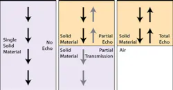
In reflection-mode imaging, the second type, the scanning transducer pulses ultrasound into the component and receives the return echoes a few millionths of a second later (Figure 1). Gaps have the highest amplitude (white in monochrome images), and normal material boundaries have medium amplitude (gray). Echoes generally are selected by their arrival time at the transducer to image a specific depth of interest.
Figure 1. Reflection-Mode Imaging
Ultrasound pulsed into a sample by the transducer of a C-SAM Acoustic Micro Imaging System is reflected 1) not at all by a homogeneous solid, 2) partially by a solid-to-solid interface, 3) almost totally by a gap.
For thorough analysis, components are imaged in both transmission and reflection modes. In commercial applications where requirements are less rigorous, the transmission mode alone might be used, for example, to find defects larger than a user-specified area.
Components across the whole range of reliability levels are imaged in one or both of these modes, which also can be performed simultaneously. The acoustic images for a military or aerospace component may look much like the acoustic images for a similar commercial component. In fact, the two components may be identical since the military has long been required to purchase commercial-grade components. But behind the scenes, there are substantial differences:
-
Commercial parts usually are shipped to the Sonoscan laboratory while military and aerospace parts are sometimes hand-carried to the lab, often by two engineers from the manufacturer who are accompanied by a government inspector.
- Military and aerospace parts typically have already been tested in other ways, including electrical tests and, for some hybrid parts where lid seal integrity (Figure 1) matters, die-penetrant tests.
- Military and aerospace personnel require absolute repeatability in the acoustic imaging protocol.
- The pass/fail criteria may be very different. A commercial part may pass if it simply has no internal defect larger than a specified area defined by the user. Military and aerospace specs often are more precise and demanding.
Many military components have a lid or container that seals the electronics from moisture, dust, and other external threats to reliability. The integrity of the seal often is the subject of acoustic investigation.
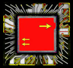
Figure 2 is the acoustic image of a PGA having a multilayer ceramic structure. This is not necessarily a military component, but it shows what can go wrong with a lid that covers the die. In this image, gaps are red. The red square at the center is not a defect but the image of the metal-to-air interface on the inside of the lid over the die. The grey border of the lid shows its seal to the substrate. Near the upper right, a red delamination (large arrow) extends through the mostly gray (= well-bonded) seal nearly to the exterior, and there are numerous smaller red defects (smaller arrows) in the lid seal. There also are red cracks between some of the leads extending from the die cavity; these can cause shorts. Red delaminations also occur on the pads beneath the leads. Conclusion: This ceramic component would not be a good choice for a high-reliability application.
The gray square at center is the lid seal in this PGA. But parts of the seal show red gaps where there should be none. The air-filled cavity under the lid is the large red square.
Imaging of components on a tray is chiefly a process of screening—that is, making an acoustic image of each part on a tray and comparing it to a defined standard. In plastic-packaged ICs, the IPC/JEDEC standard permits delaminations between lead fingers and the mold compound as long as no delamination extends more than two-thirds the length of the lead finger.
In some cases, however, screening may be followed by analysis. For example, a plastic BGA that shows internal damage may be imaged with an acoustic surface flatness module to determine whether it is warped and whether warpage may have caused the internal damage that was seen acoustically. The same module can measure the flatness of a PCB.
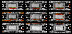
Figure 3 is the reflection-mode acoustic image of a portion of a tray of plastic-encapsulated ICs. Defects (gaps) are red. Numerous lead fingers are delaminated from the mold compound, and there also are delaminations on the die paddle. Some of these components might be usable in commercial applications. The component at the lower left could be acceptable in some military applications since it has no delaminations that exceed the 020D limitation of two-thirds of the length of the lead finger. Probably all of the others would be rejected by the same rule, in part because some of the lead fingers are very short.
Red delaminations along lead fingers and on the die paddle make most of the plastic-packaged ICs on this tray rejects.
Conclusion
Makers of components have, in some cases, initiated their own post-production acoustic inspection systems. This is true in the case of ceramic chip capacitors where the manufacturer may image a percentage of the capacitors in a lot to make sure defects are not numerous. The manufacturer may even image 100% of the capacitors in a lot, but the MIL/Aero user of the capacitors still is likely to send them to a lab for verification—and the lab may well find defects because it is an independent operation, uses stricter imaging protocols, and devotes more time to each component.
Such an approach is helpful in finding, for example, small voids in multilayer ceramic chip capacitors. If there is a void within a dielectric layer in a ceramic chip capacitor, tiny leakage currents may slowly coat the interior of the void with metal until a short occurs between the two metal layers.
How big the void must be to cause metal migration and electrical failure depends roughly on the diameter of the void and its location in relation to adjacent metal layers. The rule of thumb (it’s not an inspection standard) is that a void that extends more than 50% of the distance between two metal layers may create a pathway for a short. In some cases, 50% of the distance may be covered by a string of very tiny voids rather than by a single void.
There are many other techniques, specific to individual component part types, that labs use to characterize MIL/Aero components as fully as possible. Knowledge of the components and their imaging helps to provide maximum long-term reliability.
About the Author
Tom Adams is a freelance writer and photographer who has written more than 500 articles for semiconductor and microelectronics trade magazines.
For More Information
About the Author
Voice Your Opinion!
To join the conversation, and become an exclusive member of Electronic Design, create an account today!

Leaders relevant to this article:


