At the 2015 IEEE International Symposium on Electromagnetic Compatibility and Signal Integrity held last month in Santa Clara, I attended two technical presentations related to PCB power planes. One, “A Comparison of Relative Shielding Provided by Stitching Vias and Edge Plating” by Jim Chiappe at Juniper Networks, used simulations to investigate the effectiveness of single and multiple rows of vias with various spacings. The other paper, “Practical Aspects of Embedded Capacitance for Printed Circuit Board Power Distribution Networks” by Scott Piper at GM and James Teune at Gentex, mixed theory, simulations, and actual experiments to examine the effects of both embedded and conventional decoupling capacitors.
For any PCB power distribution network (PDN), the goal is to maintain the impedance below some critical value throughout the frequency range of transient currents. If this is accomplished, the end result is a system in which variations in the supply voltage delivered to the load are within some specified limits.
Piper received several comments after his presentation of the paper, many appreciative of the amount of experimental work that had been done. Nevertheless, some areas remained ambiguous. For example, when comparing the differences in results obtained from a square and a rectangular PCB, the paper stated, “…Even though the inter-plane capacitance is very similar for these two PCBs, their impedances vary at high frequencies. This shows that at higher frequency, length and width geometry is a factor…”
To better understand both papers, I did some web-based research into PDN impedance that quickly turned up work by Dr. Istvan Novak, formerly a signal-integrity engineer at SUN Microsystems and today a distinguished engineer at Oracle. In a 2006 paper, Novak partitioned PDN designs into four categories: multipole, capacitors by the decade (CBD), Big-V, and distributed matched by-passing (DMB). He described examples of each technique but also commented that “… there is no clear boundary between these design approaches; we can gradually transform one into the other by varying parameters, and there are an infinite number of variants in between.”1
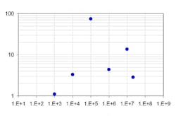
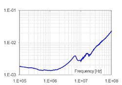
Multipole and CBD are treated together because CBD is a version of multipole. In this technique, several capacitors are used in parallel, each one having sufficiently different C and L values that the self resonances maintain the PDN’s low impedance to high frequencies. Figures 1a and 1b show an example of a CBD design.
Figure 1. Distribution of capacitance values (a) and measured self-impedance profile (b) on the V890 CPU module
Courtesy of Istvan Novak
The Big-V name describes the large dip in impedance caused by using many decoupling capacitors of the same size. Rather than a series of smaller ripples, the Big-V approach produces one large V-shaped dip at high frequency. In contrast, a design that uses DMB achieves the smallest amount of impedance variation, and Novak showed in the paper that more noise results from impedance variation than from the absolute impedance value. Therefore, as he demonstrated with a series of actual SUN PCB designs, any of the techniques can be made to work well if you understand that the goal is to minimize PDN impedance variation.
Power plane capacitance
The Piper/Teune paper highlighted the benefit of embedded capacitance. Although it concentrated on the C and L associated with the planes, it did not consider the transmission line nature of the PCB layers. In a 1998 Novak paper, an equation is derived that evaluates the approximate impedance of a power/ground-plane pair. This is the impedance that any of the four design techniques must match to minimize impedance variations.
However, Novak explained, “… Usually, the innerplane capacitance is small compared to the total bypassing needs, but the capacitance exhibits low inductance …. Unfortunately … the open boundaries at the periphery of the planes create standing waves, which in turn show up in the impedance profile of the planes as peaks and valleys at higher frequencies. With open edges, frequencies of minima in the impedance profile depend on the location of sensing points (multiples of quarter-wave resonances) while maxima are determined by the dimensions of planes (multiples of half-wave resonances).” 2
The Piper/Teune paper concluded that some of the high-frequency ripple was caused by the embedded capacitance resonating with the discrete capacitor lead inductance. Nevertheless, because the paper did not treat the inner power-ground plane pair as a transmission line, the resonance Novak discussed was not considered.
Novak’s 1998 paper described a distributed edge termination technique that eliminated power plane resonance. By adding a number of series RC networks between the power and ground planes and spaced evenly around the plane perimeter, the transmission line is effectively terminated, eliminating reflections and reducing noise.
In an interview conducted by Paul Rako at DesignCon 2014,3 Novak was asked whether Howard Johnson’s view of the technique was right—it stopped the planes from oscillating—or if Cisco’s Bob Thomas was right in saying that the technique killed leaking RF. Novak replied, “They are both right.” If only decoupling capacitors are used, their impedance does not match that of the power/ground plane pair, so reflections occur. Adding a resistor in series and spacing the RC networks around the plane perimeter eliminates reflections and was the subject of a 1997 SUN paper by Smith and also a 1996 paper by Lei, Techentin, and Gilbert. Novak does not claim to have discovered the idea although he used it extensively at SUN.
Several alternative approaches can accomplish similar results. In the 1998 paper, Novak stated, “… The inherent dielectric losses of FR4 and [similar] materials together with the copper losses do help to some extent, but those losses [alone] won’t reduce resonances sufficiently. In other solutions, highly lossy dielectric materials are used.” This thought was discussed in more detail in part of the 2014 interview as well as in the 2006 paper. In the interview, Novak said, “The plane termination technique was very useful in the late ‘90s and early 2000s when many boards had large continuous power and ground planes prone to strong resonances. However, as system density continues to grow, we are now forced to chop up power plane layers into many smaller puddles. Under these circumstances, using edge termination becomes less attractive. If resonances are still making problems, a better way [is to use] very thin laminates.”
FaradFlex, made by Oak-Mitsui Technologies, is such a material and available in thicknesses of 8 µm, 12 µm, and 24 µm with capacitance at 1 MHz of 3.1, 1.9, and 1.2 nF/inch2 for standard Dk material, and 7.1, 4.2, and 1.7 nF/inch2 for high Dk products, respectively.
Examples
In the 2006 paper, Novak described the performance of a 4-inch x 6-inch PCB designed in the mid-1990s for the E450 server that used a multipole approach. It had two major supply rails and 351 bypass capacitors with 17 different values. He commented, “The finite granularity of available capacitance, ESR, and ESL values results in unequal [impedance] peaks and valleys. ESR of MLCC parts with several µF and higher capacitance is approaching a couple of milliohms, making synthesis of 10 milliohms and higher target impedances difficult.”
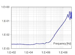
The next example was a V890 server 10-inch x 20-inch board designed in the early 2000s. It provided eight supply rails and used 1,907 bypass capacitors with six values to implement the CBD approach (Figure 1a). He said, “Low-Q bulk capacitors were complemented by a set of 10-µF and 1-µF MLCC parts …. Note that the [impedance] minima from MLCCs do not go deep; this minimizing the transient noise (Figure 1b).”
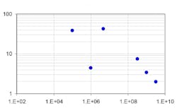
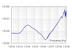
Finally, Novak considered the T2000 CPU module board, 8-inch x 10-inch with six supply rails and designed about 2005 with 596 bypass capacitors having six values (Figure 2a). The smallest value, 0.1 µF, was used for plane edge termination and the other values for the rails: only one value was used for each rail, leading to the classic big V profile on a low-power rail (Figure 2b).
Figure 2. Distribution of capacitance values (a) and measured self-impedance profile (b) on the T2000 CPU module, low-current rail with Big-V design
Courtesy of Istvan Novak
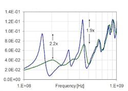
However, on a high-current rail, multiple power planes were used in the stackup. Novak explained, “A combination of horizontal plane resistance, component placement, and plane allocation made it possible to almost completely eliminate the impedance minimum at the self-resonant frequency of the MLCC parts, effectively creating a flat R-L type response characteristic to DMB (Figure 3a).” In addition, as shown in Figure 3b, very high frequency resonances were reduced when dissipative edge termination was used.
Courtesy of Istvan Novak
The point of the examples, as stated early in the 2006 paper, was the importance of achieving minimal impedance variation. Each of the designs accomplished that, but through different means.
Shielding
In the Novak interview, the interviewer, Rako, commented, “For years, engineers have put power and ground planes or two ground planes on the top and bottom of the board so it makes an enclosure, a metal can that keeps the signal traces inside from radiating. Those same engineers noticed that when the edges of the boards were open, RF would leak out of the edges and cause problems with signal integrity, power integrity, and EMC.”
With a ground plane top and bottom, a row of vias along the board perimeter effectively completes the shield can along the board edges. Chiappe’s simulations showed that high levels of shielding were provided by vias spaced from 5 mm to 0.625 mm apart, the tighter spacing corresponding to greater shielding at high frequencies. Nevertheless, because multiple PCBs are produced within a standard size blank, there are small break-off areas between boards that are susceptible to RF leakage unless the row of vias continues across the area.
Simulations also were performed for edge plating, which provides even better shielding than via stitching, but cannot be used along the break-off areas. Here, vias must be used to complete the shield. Edge plating also is unsuitable for boards that slide in guides because the plating is not mechanically robust.
In terms of cost, extra vias don’t appear to increase PCB cost appreciably. As Chiappe noted, it depends on the drill breakage rate and whether you need to have exceptionally small vias. On the other hand, edge plating did add extra cost.
No doubt, there are many design constraints that determine whether a Faraday-cage approach makes sense in a given application or whether terminated power/ground planes and very thin embedded laminates, as advocated by Novak, are a better choice when controlling PDN emissions.
References
- Novak, I., “Comparison of Power Distribution Network Design Methods: Bypass Capacitor Selection Based on Time Domain and Frequency Domain Performances,” DesignCon 2006.
- Novak, I., “Reducing Simultaneous Switching Noise and EMI on Ground/Power Planes by Dissipative Edge Termination,” 7th Topical Meeting on Electrical Performance of Electronic Packaging, 1998.
- Rako, P., “Istvan Novak on power integrity,” Bits and Pieces from the Embedded Design World, Feb. 28, 2014.
About the Author
Voice Your Opinion!
To join the conversation, and become an exclusive member of Electronic Design, create an account today!

Leaders relevant to this article:

