As the digital semiconductor manufacturing process moves into the FinFET era, more and more front-end-of-line (FEOL) defects are observed due to extremely small feature size and complex manufacturing processes required. These FEOL defects tend to manifest as cell-internal or transistor-level defects, which become big challenges for physical failure analysis (PFA) and yield analysis because traditional yield-learning methods become less effective. Furthermore, it has been shown that fin-related defects, like fin stuck-on, fin stuck-open, and gate-oxide short, tend to be timing-related because of the unique FinFET transistor structure, and thus even more challenging to identify.1
To find defect locations in failing digital ICs, product engineers typically use the established software-based methodology called scan test diagnosis. Using structural test patterns (such as ATPG) and the design description, diagnosis turns failing test cycles into valuable data. Until now, scan test diagnosis has only been able to differentiate between defects in cells and interconnect. However, a novel technology to perform transistor-level diagnosis, called cell-aware diagnosis, can identify both static and timing-sensitive defects inside standard cells. This arms yield, product, and failure-analysis engineers with an effective tool that simplifies the tasks of locating defects and identifying systematic defects of the type that is on the rise in FinFET processes.
Cell-aware diagnosis is made possible by a new type of fault model. These fault models are created by analog simulation for all physical defects extracted from the library cell layout.2 These models are used during diagnosis, along with the design description, tester failure data, and the test patterns.
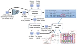
Cell-aware diagnosis works for any scan ATPG pattern type, such as stuck-at, transition-delay, and cell-aware. The diagnosis reports list the best matching suspects with the layout information after considering both interconnect suspects and cell internal suspects. The comprehensive layout picture from the proposed list of suspects covering both interconnect defects and cell internal defects is helpful for guiding the PFA process and performing yield learning. The cell-aware diagnosis flow is illustrated in Figure 1.
The generation of the cell-aware fault model is a one-time task per technology. Once created, this fault model can be used for both test-pattern generation and diagnosis for any design based on that technology. The input to the fault-model creation step is a Spice netlist including X/Y location and layer information of each object in the Spice netlist or the layout file of each such that the Spice netlist can be extracted from it. Outputs of this characterization step are the cell-aware test and diagnosis model for all cells in the technology library. In addition, layout marker files for each cell enable easy cell-level viewing of internal suspects in the layout. Timing-related defect-specific issues like passing bit mismatch and glitch excitation are properly considered as well.
To enable an accurate diagnosis, the layout of the cell is taken into consideration just as is done for layout-aware interconnect diagnosis.2 During the fault-model generation process, the critical area and the related defect probability of each potential bridge and open defect are analyzed. A high probability is reached when the distance of the adjacent nets is just one technology length and the length of the bridging area is, for example, 10 or more technology lengths. A low probability is present when the bridging length is just one technology length and the distance of the adjacent objects is, for instance, 10 times or more the technology length.
An analog simulator then is used to simulate each potential defect against an exhaustive set of stimuli to determine if there are sets of cell inputs that produce an output sufficiently different than the defect-free result.
The final step in the cell-aware fault-model analysis process is to convert the list of input combinations into a set of the necessary input values for each fault within each cell. Because this information is defined at the cell inputs as logic values, it is basically a logic fault model representation of the analog defect simulation. This set of stimuli for each cell represents the cell-aware fault model file for ATPG and diagnosis. Within this file, a simulated defect (now a fault) can have one or more input combinations.
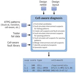
Once the cell-aware fault model is created, the cell-aware diagnosis flow is virtually identical to the one of traditional layout-aware diagnosis. As Illustrated in Figure 2, the gate-level (flat model) and layout descriptions (layout database) of the design are read into the diagnosis tool along with the test patterns. The only unique step to enable cell-aware diagnosis is to also read in the cell-aware fault models. For a given failure file, the cell-aware diagnosis algorithm first tries to find initial candidates by path-tracing every failing pattern, and it creates suspects by simulating failing patterns to find failing pattern matches. Cell-aware diagnosis creates another set of suspect cell instances based on the cell-aware fault models and simulates the failing patterns for them. Then passing patterns are simulated on both suspect lists before these are merged in a way that identifies the best matching symptoms and suspects. Timing-related defect-specific issues like passing bit mismatch and glitch excitation are properly considered as well.
The cell-aware diagnosis algorithm simulates cell internal defects directly at the gate level by using the accurate defect models derived by the analog simulator. This improves the diagnosis quality by avoiding the heuristics-based excitation condition extraction. Another benefit is that it can properly handle complex cell internal defects with non-stuck-at behavior.
Cell-aware diagnosis can pinpoint the potential defect location inside the suspect cell, such as an open defect at a specific transistor, a short between two polygons, etc. Beyond the typical diagnosis report, which lists all callouts for both interconnect and cell-internal defects, a chip-level layout marker file can be generated to highlight all potential defect locations for guiding the PFA process. The cell-aware diagnosis reports can be used for volume yield analysis similarly to how traditional reports are used.
Several cell-aware diagnosis results have been published based on technologies from 160 nm down to 14-nm FinFET.1-4
In reference 3, several diagnosis results from an AMD APU manufactured in a 28-nm process were compared with PFA results to compare diagnosis accuracy and resolution. One of these is a defect within a scan flip-flop. This device passed chain tests but failed scan tests. Regular layout-aware diagnosis called out a scan flip-flop cell and its SEN input pin. This scan flip-flop cell has 38 transistors. Cell-aware diagnosis called out 13 cell-internal suspects out of a total of 350 defined fault locations inside the cell. The 13 suspects included one transistor stuck-on, one transistor stuck-off, five bridges, and six open faults. That corresponds to a resolution improvement of 350/13 = 27X.
A close look at these suspects reveals that the majority (10 out of 13) are connected to one cell-internal net, and the other three suspects are connected to a second net, both connected to the same transistor. The real defect found by PFA is shown in Figure 3 next to the cell layout. The defect was an unlanded contact at the location which is circled in red in the layout. The open suspect S1.6 from cell-aware diagnosis (highlighted in red) covers this open contact.
In all of the 17 cases examined in this experiment, the actual defect was included in the diagnosis results. On average, the diagnosis resolution for cell internal defects was improved by 11.3X.
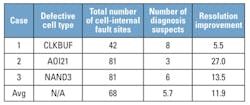
In reference 1, several real failing silicon chips manufactured in a FinFET technology with known timing-related defects identified by PFA were used to validate the proposed methodology. These dies passed static tests and failed at-speed tests only. For all three cases, cell-aware diagnosis correctly called out a cell-internal delay defect which matches the real defect found by PFA, and the bounding box for this callout properly covers the real defect. The resolution improvement is summarized in Table 1. For example, for case 2, the traditional delay diagnosis calls out defective cell AOI21 with a total of 81 cell-internal faults.
Cell-aware diagnosis reduced the size of this list down to three cell-internal suspects and thus speeds up the PFA process. For all the cases in reference 1, cell-aware diagnosis on average reduced the number of cell-internal suspects by greater than 11X compared to traditional delay diagnosis.
Cell-aware diagnosis has been validated successfully on several real silicon failures with known PFA results. The diagnosis resolution for cell internal defects can be improved by up to 70X on a complex full adder cell, and by over 10X on average, with a small time overhead. Cell-aware diagnosis is enabled by a layout-justified cell-aware fault model, which is generated once per library. Therefore, there is no impact on the data collection and diagnosis flow. Cell-aware diagnosis improves results for single-part diagnosis scenarios such as customer return analysis as well as volume diagnosis applications like yield analysis.
About the author
Geir Eide is a product marketing director in the Silicon Test Solutions group at Mentor Graphics Corp. He earned a B.S. and an M.S. in electrical and computer engineering from the University of California at Santa Barbara. [email protected].
References
- Tang, H., et al., “Diagnosing Timing Related Cell Internal Defects for FinFET Technology,” International Symposium on VLSI Design Automation and Test, 2014.
- Maxwell, P., et al., “Cell-Aware Diagnosis: Defective Inmates Exposed in their Cells,” European Test Symposium, 2016.
- Tang, H., et al., “Diagnosing Cell Internal Defects Using Analog Simulation-based Fault Models,” Asian Test Symposium, 2014.
- Tang, H., et al., “Diagnosing Cell Internal Defects for FinFET Technology,” Poster, IEEE International Test Conference, 2016.
About the Author

Geir Eide
Voice Your Opinion!
To join the conversation, and become an exclusive member of Electronic Design, create an account today!

Leaders relevant to this article:


