Designing Power ICs in an Application-Specific Automated Test Equipment System

What you’ll learn:
• Meet custom load current requirements in device power supply
• Increase output current
• Choose the correct heatsink for a DPS system
Device power supply (DPS) ICs have flexible force voltage and force current capacities to provide dynamic test capabilities to automated test equipment (ATE). The DPS IC is a voltage source when the load current is between the two programmed current limits and gracefully transitions into a precision current source/sink when a programmed current limit is reached.
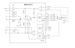
Figure 1 shows the simplified architecture of Maxim Integrated’s next generation device power supply, the MAX32010. Switches FIMODE, FVMODE, and FISLAVE MODE select different modes such as FV (Force Voltage), FI (Force Current), and FI Slave Select whereas switches HIZF and HIZM select the MV (Measure Voltage) and MI (Measure Current) modes, respectively. RANGE MUX allows for multiple current ranges RA (1.2A), RB (20mA), RC (2mA), and RD (200µA) in combination with external sense resistors. Custom current ranges can be designed by changing the sense resistor value, using the formula RSENSE = 1V/IOUT. The CLEN switch and both ICLMP and VCLMP DACs allow the user to set programmable voltage and current clamps.
This article first covers two important considerations when designing a Device Power Supply IC into a system, Range Change Glitch and efficiency. Later, the article details some aspects of building a DPS system to meet application-specific requirements.
Range Change Glitch:
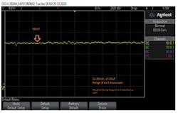
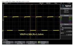
Let us look at the first consideration, Range Change Glitch. While the ATE is performing the DUT testing, the system might need to change the current range for different tests. IDDQ or quiescent current measurements usually require the lowest current range for measuring smaller values of current. A voltage spike or glitch while moving to the lowest current range can not only affect the measurement but also possibly damage the DUT. Glitch-free range changing protects the DUT and validates the test.
When testing with a load capacitor of 270pF, Maxim Integrated’s DPS performs this transition smoothly, as shown in Figure 2. Without a load capacitor (0pF), this transition happens over a span of 20µs with ramp rate of 25mV/20µs. This transition is much smaller than the competition’s glitch during transition. The competition’s DPS has a glitch of 159mV over a period of a few microseconds. In this example, Maxim Integrated’s DPS performance is 536% better than the competition’s range change performance without causing any damage to the DUT.
Device Power Supply Efficiency:
Device power supply efficiency is the second important consideration when choosing your DPS IC since it directly affects the cost savings and the reliability of system. The greater the efficiency, the greater the cost savings, reliability, and oftentimes the longevity of the system. The less efficient the DPS, the more heat is generated; more heat means more wear and tear and a higher failure rate of components in the system.
Device power supply efficiency is calculated as Efficiency = Power output/Power Input.
As shown in Table 1, Maxim Integrated’s DPS supplies more current (1.2A) than the competition’s DPS (1A) at a higher efficiency (58.33%). Maxim Integrated’s DPS efficiency is 11% better than Competitor 2’s DPS IC and 155% better than Competitor 1’s.

How to meet Custom Load Current Requirements in DPS
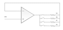
Each ATE has custom load current requirements with respect to each device under test (DUT). The MAX32010 enables custom range selection by changing only one sense resistor value. The RANGE MUX in MAX32010 selects one of the following current ranges: RA (1.2A), RB (20mA), RC (2mA), or RD (200µA).
The sense resistor value is chosen by using the following formula, RSENSE = 1V/IOUT. For example, the load current requirement is 5mA; 5mA is a custom load current, which falls under Range B. To choose the correct RSENSE: RSENSE = RB = 1V/5mA = 200Ω. Refer to Maxim Integrated’s application note 7068 for more details on the selection of sense resistors (Figure 3).
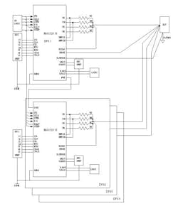
Many times, the DUT might require higher current than a DPS can supply. Excess current over 1.2A can be achieved by connecting multiple DPS devices in parallel as shown in Figure 4. Both devices are kept in FI mode to double the current. As an example, connecting two 7V, 1.2A devices together in parallel can achieve up to 7V, 2.4A of output current.
Another way to increase the output drive current capabilities of DPS is to pulse the output. If the current requirement is only for a short duration, then pulsed testing is a viable option as shown in Figure 5. One possible example of this test is I-V characterization of DUTs. Pulsed testing is done by changing the duty cycle of FI ON Time.
In this test, DPS mode is set to FI mode for 50% of the time and “High Impedance” mode is set for the other 50% of the time. The duty cycle can be varied as per the DUT current requirements. We have performed this experiment on the MAX32010 IC and the result is as follows:
Maximum output current = 1.436A with up to 50% duty cycle
How to Choose the Correct Heatsink for DPS System
It is imperative to choose the right heatsink for a reliable and stable system. The following example shows a step-by-step guide to choose the correct heatsink for the MAX32010.
Step 1: Obtain the package’s relevant dimensions. Thermal analysis of the package helps to choose the correct heatsink. It is important to understand the area of the exposed pad for heat dissipation.
Step 2: Get PCB thermal properties to calculate boundary conditions for theta-JA. Calculate the power loss and consider all mediums for dissipation of heat (conduction, convection, and radiation).
Step 3: The heatsink base area and flow rate of the heatsink fan are two variables that are important when calculating the temperature distribution of the package. Keep in mind that the junction temperature of the IC should remain below the thermal shutdown temperature. Our analysis using still air shows that a heatsink with a base area of 30.48mm x 30.48mm, a thickness of 5mm, and 15mm long fins are required to maintain junction temperature below 140°C for the MAX32010 (Figure 6).

Step 4: Airflow and heatsink material also play an important role in keeping the junction temperature of the IC below 140°C. Our analysis shows that a significant improvement in temperature performance was achieved by adding 1m/s of airflow to the Cu heatsink.
Conclusion
This article provides guidelines for selecting the device power supply (DPS) IC in automated test equipment (ATE) system. These considerations will help customers to select the DPS IC as per their specific ATE system. The article also explains the system-level architecture to tackle the output current and thermal requirements of the ATE system
About the Author

Madhura Tapse
Madhura Tapse joined Maxim Integrated as Member of Technical Staff in 2016 and has worked on various product families such as, supervisory ICs, power monitoring ICs, interfaces ICs and ATE ICs. Prior to joining Maxim, Tapse worked as an applications engineer at Cypress Semiconductors. She holds a Bachelor of Science degree in Electrical Engineering from Pune University and master’s degree in Biomedical engineering from Indian Institute of Technology, Bombay.
Comment About the Article
To join the conversation, and become an exclusive member of Electronic Design, create an account today!

Leaders relevant to this article: