Real Time Waveform Analysis Helps Optimize Charger Performance
Find a downloadable version of this story in pdf format at the end of the story.
Today, cell phone charger designs face many technical challenges, including increasingly stringent technical, cost and size requirements driven by end users, OEMs of handheld devices, cell phone charger manufacturers, and regulatory agencies. This has created an opportunity for the development of next generation power supply controller technologies that take full advantage of real-time signal examination and control techniques.
Cell phone chargers allow normal operation of the handheld device while connected to the ac voltage source. Fig. 1 shows the typical cell phone operating modes that provide a regulated constant voltage (CV) output, VOUT. Here, output voltage is sensed directly and the feedback signal transferred to the primary controller via an opto-isolation device.
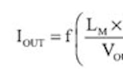
Besides the “operating mode,” cell phone chargers manage the charging function of the battery (typically Li-ion) of the handheld device. Again referring to Fig. 1, the “charging mode” provides a regulated constant current (CC) output IOUT, which requires sensing of the output current. Again, this can be provided by current sense circuit on the secondary side. Alternatively, primary-only constant current regulation can be achieved using two well known methods: the power balance equation (Equation 1), or the time average equation (Equation 2).
Where:
f = Function of
IOUT = Output current in Amps
LM = Magnetizing inductance in Henries
IPK = Primary peak current in Amps
VOUT = Output voltage
Where:
f = Function of
N = Transformer turns ratio
tRESET = Transformer rest time in µsec
T = Switching period in µsec
Using the power balance equation, output voltage regulation is critical because it has a direct bearing on constant current performance. Likewise, using the time average requires an accurate measurement of transformer reset time.
Continue on next page
NO-LOAD POWER DISSIPATION
Typically, cell phone chargers connect to the handheld device only for the purpose of charging the battery. The majority of time cell phone chargers remain connected to the ac voltage source without any load. This wastes a large amount of energy, based on many millions of cell phone chargers connected to the ac voltage source at any given time. To minimize waste, cell phone chargers are subject to compliance of various regulatory and industry based requirements.
For example, Energy Star requirements for ac - dc power supplies specify the maximum power a cell phone charger can dissipate under no-load conditions. This is while maintaining proper output regulation to prevent any damage to the handheld device when re-connected to the charger. Under the Energy Star V2.0 (level V) the no-load consumption of a typical charger must be less than 300 mW at 230Vac input. In November 2008, the world's five largest mobile phone makers - Nokia, Samsung, LG Electronics, Motorola and Sony-Ericsson - announced the five-star energy-rating system to help consumers easily identify the most energy-efficient chargers. Under the five-star system, chargers get no stars for no-load power consumption greater than 500mW, and up to five stars for less than 30mW.
Although technical challenges for cell phone chargers have increased, pressure to reduce the unit cost has become more intense. Considering the number of cell phone chargers manufactured, any design sensitivities to manufacturing process and/or component tolerances is magnified. It is understandable that there is a focus on the bill-of-material (BOM) cost, but it is not the only factor that makes up the final unit cost. Production yield is another critical factor in determining final unit cost, and it is desirable for a cell phone charger design to be tolerant of a wide range of manufacturing and component variability. If a design were to require a narrow manufacturing process or stringent component tolerance, it forces the cell phone charger manufacturer to decide between higher manufacturing fall-out or a higher BOM cost.
PROMISE OF PRIMARY-ONLY REGULATION
Although primary-only regulation can reduce BOM cost and size, early primary-only designs failed to meet the performance targets needed for cell phone chargers. Fig. 2 shows the feedback provided by an auxiliary winding of the power transformer. This design fails to meet the output voltage regulation performance because it is susceptible to cross regulation variation between the feedback output and the main output. Furthermore, it requires secondary output current sensing, which eliminates any advantage of primary-only regulation.
Fig. 3 describes the performance characteristics of the dc sensing implementation. As described above, the wider variation of the output voltage has a direct bearing on the constant current regulation as well as the wider variation of the CV to CC transition point.
There was a widely-held belief that primary-only regulation is a trade-off between performance and cost. However, real-time digital techniques allow cycle-by-cycle examination of ac waveforms, which allow precise monitoring and control of critical power supply parameters. As a result, primary-only control results in improved performance, reduced BOM cost, greater manufacturability, and precise protection against fault conditions. Fig. 4 illustrates key monitoring points, while Fig. 5 describes the associated operational waveforms.
Continue on next page
Control signal controls the ON and OFF state of the power transistor. While in the ON state, primary current starts to ramp up through the primary magnetizing inductance of the power transformer. The secondary rectifier is reversed biased, and energy is stored in the air-gap of the power transformer. When the power transistor is set to the OFF state, the secondary rectifier is forward biased and energy from the power transformer is delivered to the secondary load. When the power transistor is initially turned to the ON state, there is a voltage spike and ringing caused by the “miller-effect” the power transistor. When the power transistor is turned to the OFF state, there is a high voltage spike and ringing caused by the leakage inductance and the parasitic capacitance of the transformer.
The cycle-by-cycle sensing of the VSENSE signal allows for a suitable proxy for the output voltage due to the following relationship:
Where:
NAUX = Turns in auxiliary winding
NSEC = Turns in secondary winding
NAUX / NSEC = Power transformer auxiliary to secondary turns ratio
VOUT = Output voltage
VDROP(ISEC) = Voltage drop across secondary rectifier diode, function of the secondary current, ISEC
ISEC = Secondary current in Amps
RSEC = Secondary parasitic resistance including winding resistance and PCB trace resistance in ohms
NON-OPTIMAL IMPLEMENTATIONS
A non-optimal implementation of primary-only regulation using ac waveform sensing encompasses the sensing of the VSENSE waveform using a fixed time period (TFIXED), between the OFF strobe of the control signal and the sample time (tSAMPLE). Fig. 6 illustrates that feedback signal VSAMPLE is determined by sampling waveform VSENSE at tSAMPLE.
The period of TFIXED has to be selected very carefully. If it is too short, the signal integrity of the VSENSE waveform will be corrupted by the flyback noise. Furthermore, the term from Equation (3):
will be large due to the high level of secondary current at time tSAMPLE, and will have a large variability from cycle-to-cycle. However, if TFIXED is too small, the reflected voltage portion of the VSENSE waveform will be too short under light load conditions to obtain an accurate reading of the output voltage via VSAMPLE. Fig. 7 shows this condition.
Besides these design constraints, the unit-to-unit performance will be directly dependent on the variability of key components, including, the power transformer leakage inductance, power transistor gate capacitance, forward voltage drop of the secondary rectifier, and impedance characteristics of the output filter stage. Lastly, this implementation is also more susceptible to cross regulation variations
Continue on next page
Although cycle-by-cycle sensing the VSENSE waveform using a fixed time represents a significant improvement over dc waveform techniques, the factors above highlight the limitations of this approach, especially in high volume applications, such as cell phone chargers, where it is desirable to have a design that is insensitive to manufacturing processes and component variations.
Fig. 8 describes the performance characteristics of the non-optimal implementation. Furthermore, as described above, the wider variation of the output voltage has a direct bearing on the constant current regulation as well as the wider variation of the CV to CC transition point.
NEXT GENERATION MYTH BUSTER
Next generation digital waveform analysis and control techniques are being introduced to remove the performance and manufacturing limitations from those found in legacy products. By using the power of adaptive waveform analysis, it is possible to provide superior performance and lower cost.
Fig. 9 illustrates that the VSENSE waveform is sampled at the VSENSE knee. Furthermore, VSAMPLE is taken at the VSENSE knee on a cycle-by-cycle basis. The VSENSE knee occurs when all of the energy from the power transformer has been delivered to the secondary.
Once again using Equation (3), we can see what is unique about this particular point of the VSENSE waveform. As all of the energy from the power transformer has been delivered to the secondary, the secondary current approaches 0 Amps. This is also referred to as the transformer reset point. You will notice that the variable term based on the secondary current is minimum, because generally the forward voltage drop across the diode reduces if the conducting current is lower. Only at this point, the VSENSE signal is exactly equal to the output voltage multiplied by the power transformer turns ratio plus the rectifier diode forward voltage drop at zero secondary current. The rectifier diode forward voltage at zero secondary current is minimum at this point and thus can be ignored as such.
At VSENSE knee: VSENSE = (VOUT) × (Turns Ratio)
Adaptive cycle-by-cycle sampling at V-sense knee is not susceptible to historically troublesome signal corruption such as leakage inductance spikes. Furthermore, as the secondary current at the V-sense knee is equal to 0 Amps, any variations in forward voltage drop across the secondary rectifier and secondary impedances will not negatively impact output regulation characteristics.
Fig. 10. illustrates that the ability to accurately monitor the transformer's “real” output voltage on a cycle-by-cycle basis is the key to achieving superior CV and CC regulation performance. This ensures that high performance can be attained in high volume cell phone charger manufacturing applications.
Download the story in pdf format here.
About the Author
Comment About the Article
To join the conversation, and become an exclusive member of Electronic Design, create an account today!

Leaders relevant to this article: