Low Noise Alternatives to Linear Regulators
Numerous electronic components like phase-lock loops, FPGA transceivers, and precision op-amps require a low noise voltage rail in order to operate as specified. More often than not, when a need for a quiet voltage rail arises, a designer reaches, almost instinctively, for a linear regulator. This choice is often made with the idea that a linear regulator is a reliable and simple means of generating a low noise voltage rail. The key parameter of the linear regulator that emboldens this confidence is the power supply rejection ratio (PSRR). The PSRR is a metric of how much input power supply noise the linear regulator will reject and how quiet the resulting output is expected to be. If properly selected, a linear regulator can be a good solution, but if not, the result can be an output voltage rail that’s noisier than desired and dissipating unnecessary power.
Selecting a linear regulator for a low noise voltage output relies on an accurate evaluation of the PSRR specification. Doing so allows a designer to estimate, with some confidence, the amount of input noise that will appear on the output. The PSRR of a linear regulator is characterized by imposing a sinusoidal signal on the DC input voltage and varying the frequency of this signal over some range and measuring the amplitude of the signal that is passed through to the output. The result is a ratio of the output signal over the input signal expressed in decibels (dB). The bandwidth limitation of the linear regulator’s internal error amplifier results in a PSRR that rolls off with frequency as shown in Fig. 1. This means it will attenuate low frequency noise better than higher frequency noise.
Power supply rejection ratio
The majority of higher current linear regulators have PSRR curves that are near 0dB above a few hundred kilohertz and this is especially true for linear regulators that can source more than 0.5A. Therefore, a designer needs to evaluate the PSRR of a regulator while keeping in mind the amplitude and frequency of the voltage ripple and noise on the regulatorís input. Often, the PSRR is considered only as a line item on a regulator’s datasheet which is often specified at 1KHz or worse yet 120Hz, harkening back to a day when the rectified output of a 60Hz transformer supplied the DC input to the linear regulator. Whereas the actual switching frequency of the power supply, and resulting voltage ripple, on the input of a linear regulator typically has a frequency that is higher than 1MHz and switching related noise that can easily be over 100MHz.
Even the best linear regulator will have a difficult, if not impossible task, generating a quiet output voltage if noise on its input is greater than 10MHz. To maximize the performance of a linear regulator itís beneficial if the switching frequency of the upstream switch-mode power supply is as low as possible. Additionally, filter any high frequency noise before it reaches the linear regulator, and finally select a regulator with the best high frequency PSRR available for the quietest output possible.
An alternative can be a switch-mode power supply (SMPS) that generates very little noise in the first place. Significant improvements have been made in the design of many voltage regulators and power modules that make them capable of a quiet output voltage which can rival or even best a linear regulator. This ability is achieved in part by improvements in power semiconductor design and packaging as well as on-chip inductors. Since any SMPS will have some level of output ripple and noise, the key is selecting a supply that generates minimal voltage ripple/noise and applying some simple ideas to further quiet the output voltage. The printed circuit board layout of a SMPS can also contribute to minimizing the amplitude of output noise; discussions on layout related noise mitigation is available in applications notes AN-1950 and AN-2078 at national.com.
Ideally, a quiet voltage rail has an output which is exactly equal to the desired voltage level with no measurable deviation over time. Any noise is then simply unwanted variations in the output voltage. Power supply designers often differentiate the output noise based on what generated it like voltage ripple and switching related noise. But that matters very little when the load simply needs a quiet voltage rail that is typically specified as a percentage of Vout or simply in voltage amplitude with no consideration of the frequency or source of the noise. However, understanding a little about the source of the noise will help in minimizing it.
Minimizing output ripple
The output ripple of a SMPS is largely a function of the inductor ripple current and the ESR of the output capacitor(s). Selecting low ESR output capacitors will minimize the voltage ripple, and so will increase the value of the storage inductor and the switching frequency. If a power module is selected, many of these decisions are resolved in the design; however, the need for low ESR output capacitors remains. The switching-related noise on the output of a SMPS is the linked to the switching of the power MOSFETs and is passed to the output by the parasitic capacitance of the storage inductor. This noise, which shows up as voltage spikes, looks like “ringing” with a frequency that is much higher than the FSW and can be well above 100MHz. The voltage ringing shown in Fig. 2, was measured on the output of a 1A, SMPS and has a frequency of about 500MHz. The amplitude of this noise can be attenuated by placing a properly selected bypass capacitor at the output in addition to the larger value output capacitors to filter the noise. The value of the bypass capacitor can be selected by first measuring the frequency of the ringing of the output noise, and then using the frequency data to calculate the capacitor value.
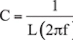
The equation for the resonant frequency of an LC circuit is rearranged to solve for capacitance (C):
Where:
f = Frequency of the noise (voltage ringing)
L = Estimated parasitic inductance as in the capacitor and PCB layout.
For example. the measurement in Fig. 2 shows a frequency of about 500MHz and using a value of 1nH (a reasonable estimate provided the capacitor is placed very close to the output pins of the module and ground and the traces in the layout are kept short) would suggest a capacitor value of 100pF. Keep in mind this is an estimate and the value of this capacitor may need some adjustment to empirically determine the optimal value. It’s also a practical idea to use a small package for this capacitor like a 0402 or 0603 to minimize the parasitic inductance associated with the part itself. Another (and possibly simpler) option for determining the value of this capacitor is to use a reactance Nomograph which plots capacitive and inductive reactance on a log scale. This method has long been a favorite of veteran analog engineers, given a nomograph is often within an arm’s reach at the lab bench or desk. Either way, this is a simple and effective method to reduce the voltage spikes on the output of a SMPS.
As mentioned, selecting a SMPS that produces minimal noise is an important first step. There are numerous options available; however, a power module offers several advantages given veteran power designers have optimized the solution. Texas Instruments has a series of power modules which have very quiet outputs and are also small and highly efficient. This is especially true of the LMZ10501 and LMZ10500, power modules which are exceptionally quiet by design. These little buck regulators have integrated power MOSFETs, a built-in inductor, and require no external compensation. Also known as the Nano modules, they can source up to 1A and 650mA of output current (respectively), operate at 2 MHz, while maintaining a peak efficiency of 96%. They come in a 2.5 x 3mm, 8-pin leadless package as shown in Fig. 3. Performance characteristics for these modules are listed in Table 1.
The output of the Nano module, configured as shown in Fig. 4, with an input voltage of 5V and output voltage of 2.5V, had a measured voltage ripple and noise amplitude of 3.7mV p-p as shown in Fig. 5. This is quiet enough to power most devices which would normally use a linear regulator. The 5V input voltage is actually a worst-case condition; the output ripple and noise was measured below 3mV p-p when the input voltage was reduced to 3.3V. The values used for this measurement were Cout1 = 100pF, Cout2 and Cout3 = 10µF. The value for Cout1 was determined as noted above. Two capacitors were used for Cout2 and Cout3 to minimize the overall ESR and the resulting output voltage ripple; both 10µF ceramic, X7R. These component values may require some adjustment based on a given PCB layout and individual design requirements.
Compare the above characteristics to a 1A linear regulator with an input ripple voltage of 30mV at the switching frequency 250KHz and 50mV of switching related noise at 100MHz. In Fig. 1 the regulator would provide 15dB of attenuation at 250KHz and unspecified attenuation for the 100MHz switching related noise. Therefore, we should expect the output voltage ripple to be about 5mV p-p, and the switching related voltage spikes as much as 50mV p-p (given there’s no PSRR data above 1MHz).
Current state-of-the-art linear regulators typically don’t specify PSRR above 10MHz. Moreover, a linear regulator would have had substantial power dissipation while still not producing an output voltage as quiet as a switch-mode regulator like the Nano module. Of course, this is just an example; however, the point being that a well-selected and designed switch-mode regulator can be as quiet as or better than a linear regulator. A small device like the Nano module can enable a design with a total component footprint of less than 13mm² (excluding the area required for PCB layout for comparative purposes).
Contrast the size of the Nano module to a linear regulator like the LP38512, capable of supplying 1A, which has a total component footprint of 115mm². While small, it’s still a considerably larger solution that other linear regulators.
Low noise output
Compact power modules like the LMZ10501 and LMZ10500 can enable a very quiet voltage output with an output power density up to 300W/in² (118W/cm²) and boast peak efficiency of 96%. Power modules like these have all the design convenience of a linear regulator, but without the inherent power losses that comes with it. The Nano module’s VCON pin can also be driven with a DAC to make it a digitally programmable voltage regulator. Despite their diminutive size, they are full-featured regulators capable of sourcing up to 1A, with under-voltage lock-out (UVLO), current limit, thermal protection, integrated loop compensation and internal soft start. The Nano modules also have extremely low EMI and are compliant with the CISPR 22 class B limits for radiated emissions. Texas Instruments has a complete line of power modules in addition to the Nano modules, a few of which are listed in Table 1.
Measuring small amplitude ripple and noise as was done for this article requires some care. To learn more details on measuring small amplitude noise and ripple from a SMPS, see application note AN-2169 for details.
In addition to the Nano modules, TI also has buck Nano regulators with input voltages up to 42 V and output currents up to 2 A, and boost Nano regulators with input voltages up to 40 V and output currents up to 2.1 A. In addition, power modules like those discussed here can provide an output voltage with ripple-and-noise that rivals and in some cases bests a linear regulator. Designers who want a clean and quiet voltage rail have options that extend beyond a linear regulator, which is highly compact and efficient.
Design engineers can get a wealth of additional information on these products, their applications, and demonstration videos on Texas Instruments’ website at www.ti.com/switcher.
Related Articles
[11/2003] Low-Voltage LDO Regulators Power Portable Gear
[3/2004] Charge Pump-LDO Chip Offers Option for Generating Low-Noise Supplies
[6/2004] Linear Post Regulators for DC-DC Converters
[5/2005] LDOs See Little Drop-Off in Interest
About the Author
Comment About the Article
To join the conversation, and become an exclusive member of Electronic Design, create an account today!

Leaders relevant to this article: