Ripple Generating Circuit for Constant-On-Time Controlled Buck Converters
Traditionally, voltage mode control and current mode control have been employed widely in power management ICs. Next generation requirements of fast transient response, ease of design, and fast time-to-market have posted great challenges to power controller providers. In recent years, constant-on-time (COT) control has gained tremendous interest from DC-DC power IC suppliers, thanks to its inherent advantages over traditional control architectures.
Fig. 1 shows a buck converter with constant-on-time control. Unlike conventional voltage-mode control and current-Mode control that employ an oscillator, an error amplifier and compensation circuit, a comparator is used in the feedback loop for COT. At the beginning of each cycle, the IC initiates an on-time period when the feedback voltage falls below the reference voltage. The high-side MOSFET stays on for a fixed duration. At the end of on-time, the high-side MOSFET turns off until the feedback voltage falls below the reference. To provide an interval for current sense and PFM operation, the controller usually provides a minimum off-time. Since the error amplifier, compensation circuit, and even oscillator are eliminated, the COT features simple implementation, easy PFM operation, and superior transient response.
As a ripple-based control approach in nature, however, COT requires minimum ripple voltage on output feedback to operate properly. Research in literature has shown that the instability is due to the phase shift of the capacitive component of output ripple [1-11]. If the capacitive ripple magnitude dominates the total output voltage ripple which consists of resistive equivalent-series-resistance (ESR) ripple, capacitive ripple, and equivalent-series-inductance (ESL) ripple, double or multiple pulses per switching cycle may occur, and result in sub-harmonic oscillation at output. A common practice to address this issue is to use bulk output capacitors with higher ESR such as electrolytic, OSCON, and POSCAPs.
If the contribution of the ESR ripple surpasses the capacitive ripple, the power supply with COT will be stabilized. The downside is that the output voltage ripple will increase, which poses another challenge to power supply design. Driven by increased pressure from tight output voltage regulation, cost and size reduction requirements, power supply designers have been trying to avoid using the number of bulk capacitors, and resort to ceramic capacitors. Compared to bulk capacitors, ceramic capacitors offer significantly lower price, smaller size, and lower ESR. Importantly, with all-ceramic capacitors being used as output filters, the output ripple will be extremely low due to small capacitor ESR. To meet the minimum ripple requirement of COT all ceramic design, a ripple-generating circuit has been widely utilized. Generally speaking, too big a ripple will cause large output voltage DC regulation error and also deteriorate transient performance, while insufficient ripple may lead to instability. Therefore, optimal values for the ripple-generating circuit are needed to meet minimum ripple voltage requirement on FB pin while still maintaining stability.
Ripple-Generating Circuit
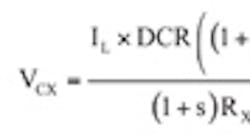
Fig. 2 shows a widely employed ripple-injecting-circuit for COT all-ceramic capacitor design. This circuit consists of a resistor and two capacitors. A resistor RX and a capacitor CX are connected to the two terminals of the inductor. If the values are chosen correctly, triangle voltage ripple will be generated on CX which resembles the inductor current ripple. The triangle voltage ripple will then be injected to the FB pin. Capacitor CD blocks the DC component of voltage on CX so that ideally only the AC ripple will pass through to reach the FB pin. In practice, the desired ripple voltage at FB pin is usually given. The ripple-generating circuit design can be started with selection of RX and CX. In the s-domain, the voltage on CX is:
Where:
IL = Inductor current
L = Inductance
DCR = Direct-Current-Resistance of the inductor
Inductor current, IL, consists of DC component that is the load current and AC component, which is the ripple current. Manipulating Equation (1) and eliminating the DC component of IL leads to the equation for the ripple voltage on Cx:
Where:
VCX(PP) = Ripple voltage on Cx
IL(PP) = Inductor peak-peak current ripple
CX is usually picked at a value in between 0.1 µF and 1 µF. When it comes to the selection of CD, a common assumption is that the ripple voltage on CX will be coupled equally to FB through CD, i.e. VCX(PP) is equal to injected ripple voltage at FB. As such, its value is chosen arbitrarily to some degree.
To verify if the above assumption is valid, a closed-loop model of COT controlled buck converter was built in Simplis. Simulation is done using two different CD values, 220pF and 1000pF, while the other parameters are kept the same. Fig. 3(a) shows the simulation results of the ripple voltages on CX and FB pin. The top window is the ripple voltage on CX, which is 11mV. Waveform 1 in red in the bottom window is the FB voltage for CD of 1000pF, with peak-peak voltage of 11mV, while Waveform 2 in green in the same window is for CD of 220pF, with peak-peak voltage of 6mV.
It was found that different CD values can result in different ripple magnitudes, even different waveform shapes on the FB pin. Therefore, the ripple voltage on CX will not necessarily be coupled to FB pin. Fig. 3 (b) shows the output voltages. Waveform 1 in red in the top window is 1.216V and Waveform 2 is 1.204V. The CD value difference alone can result in a DC regulation difference of 12mV in this specific case. Therefore, if CD is not chosen properly, the ripple voltage on FB pin can be either insufficient, which leads to instability, or too big, which not only adds DC regulation error at output but also degrades transient performance.
To better understand the effects of the CD on the FB voltage, it is worthwhile to examine the voltage on CD. If we approximate ICD(PP) as a triangle, the equation for VCD(PP) is analogical to the equation for output voltage ripple which is:
The ripple voltage on CD can be approximated as:
Where:
VCD(PP) = Ripple voltage on CD
ICD(PP) = Ripple current across capacitor CD
FSW = Switching frequency of the converter
The output capacitance value is usually large, so you can consider the output as a low impedance at high frequencies. By superposition of the ripple contributed by ripple current on CD and ripple voltage at output, the ripple voltage on FB pin is:
Based on Kirchhoff’s voltage law, the relationships of VCX(PP) , VCD(PP) , VO(PP) , and VFB(PP) are:
By examining Equation (5) we found that if VCD(PP) is made equal to VO(PP) , VFB(PP) will be equal to Vcx(pp) , which means that the ripple voltage at FB pin will resemble the triangle voltage ripple on CX under a specific condition. Therefore, if an optimal value of CD is found so that the voltage ripple on CD resembles output voltage ripple, the FB voltage ripple will be purely resistive and triangle, hence stability can be achieved under most conditions. The output ripple, CX voltage ripple, and other parameters except ICD(PP) and CD are known or obtainable from 4. Therefore, replacing VCD(PP) in Equation (3) with VO(PP) and inserting the expression of ICD(PP) into Equation (4) leads to an optimal CD value that makes FB ripple a triangle voltage:
If the number of output ceramic capacitors is big enough, the output voltage ripple will be extremely low. As a result, the injected ripple VX(PP) should be much larger than the capacitive ripple on FB pin, so Equation (6) can be further simplified to:
With the discovery of the optimal value of CD, it will appear as if the capacitive component on the feedback pin is filtered out. As a result, the ripple-generating circuit can be designed with minimum required ripple for stability, which maximizes transient performance and minimizes output DC regulation error. The design procedure of the ripple-generating circuit can be summarized as the following:
- Provide all power stage parameters.
- Determine desired injected ripple at FB pin based on controller requirements. This ripple is approximately equal to the ripple voltage on CX if the ripple circuit is designed properly.
- Pick a value for CX and calculate the value for RX by Equation (2).
- Optimal value for CD can be calculated by Equation (6).
The output DC regulation error can be approximated as:
Simulation and Experimental Results
The simulation model is built to verify the design approach for the ripple-generating circuit. The results are shown in Fig. 4. The waveforms from top to bottom are VO, VCD(PP) , VCX(PP) , and VFB(PP) . It is found that with optimal CD value, the ripple voltage on CD resembles the ripple voltage on output, hence the ripple voltage on the FB pin looks purely triangular and resistive! Moreover, the targeted injected ripple voltage (21 mV) is achieved at the FB pin.
An evaluation board was built to verify the ripple-generating circuit as shown in Fig. 5. The controller is FAN2306, which is a constant-on-time controller from Fairchild Semiconductor. The circuit parameters are:
VIN = 12V
VO = 1.2V
F SW = 500kHz
LO = 1µH
CO = 4x47µF MLCC
RT = 10kΩ
RB = 10kΩ
RX = 1kΩ
CX = 0.1µF
For the targeted 22mV ripple generated at FB pin, the calculated optimal CD is about 335pF. A 330pF standard value is chosen on the evaluation board for CD.
The experimental results are shown in Fig. 6. The top trace in green is the FB pin voltage. The yellow trace in the middle is the output ripple voltage. And the bottom trace in pink is the switching node waveform. The measured FB ripple voltage is in triangle shape with magnitude of about 24.4mV. It matches the theory fairly well.
References:
[1]Y. Lin, C. Chen, D. Chen, B. Wang, “A novel ripple-based constant on-time control with virtual inductance and offset cancellation for DC power converters,” IEEE Energy Conversion Congress and Exposition, pp. 1244-1250, Sep. 2011.
[2]C. Chen. D. Chen, C. Tseng, C. Tseng, Y Chang, K. Wang, “A novel ripple-based constant on-time control with virtual inductor current ripple for Buck converter with ceramic output capacitors,” in IEEE Applied Power Electronics Conference, 2011, pp. 1488-1493.
[3]J. Wang; J. Xu; B. Ba, “Analysis of Pulse Bursting Phenomenon in Constant-On-Time-Controlled Buck Converter,” IEEE Transactions on Industrial Electronics, vol. 58, Issue. 12, pp. 5406-5410, 2011.
[4]K. Cheng; F. Yu; P. Mattavelli, F. Lee, “Characterization and performance comparison of digital V2-type constant on-time control for buck converters,” IEEE 12th Workshop on Control and Modeling for Power Electronics, pp. 1-6, 2010.
[5]R. Miftakhutdinov, “Compensating DC/DC Converters with Ceramic Output Capacitors,” Texas Instruments Power Supply Design Seminar, 2004/05, http://www.smps.us/Unitrode.html.
[6] F. Yu, F. Lee, “Design oriented model for constant on-time V2 control,” IEEE Energy Conversion Congress and Exposition, pp. 3115-3122, 2010.
[7] J. Wang, B. Bao, J. Xu, G. Zhou, W. Hu, “Dynamical Effects of Equivalent Series Resistance of Output Capacitor in Constant On-Time Controlled Buck Converter,” IEEE Transactions on Industrial Electronics, pp. 1, 2012.
[8]R. Redl, S. Jian, “Ripple-Based Control of Switching Regulators—An Overview,” IEEE Transactions on Power Electronics, Vol. 24, pp. 2669-2680, 2009.
[9]Y. Lee, W. Lai, W. Pai, K. Chen, M. Du, S. Cheng, “Reduction of equivalent series inductor effect in constant on- time control DC-DC converter without ESR compensation,” IEEE International Symposium on Circuits and Systems, pp. 753-756, 2011.
[10]T. Shuilin, K. Cheng, F. Lee, P. Mattavelli, “Small-signal model analysis and design of constant-on-time V2 control for low-ESR caps with external ramp compensation,” IEEE Energy Conversion Congress and Exposition, pp. 2944-2951, 2011.
[11]T. Qian, “Sub-Harmonic Analysis for Buck Converters with Constant On-Time Control and Ramp Compensation,” IEEE Transactions on Industrial Electronics, pp. 1, 2012.
[12]FAN2306 datasheet, available at www.fairchildsemi.com.
Related Articles:
About the Author
Comment About the Article
To join the conversation, and become an exclusive member of Electronic Design, create an account today!

Leaders relevant to this article: