Synchronous 4-Switch Buck-Boost DC/DC Controller
Linear Techology’s LT8705 is a buck-boost switching controller that operates from input voltages above, below, or equal to the output voltage. It has four feedback loops to regulate the input current/voltage, along with the output current/voltage. On-chip quad N-channel MOSFET gate drivers control four external power MOSFETs. It is available in a 38-pin 5mm x 7mm QFN, and a 38-lead TSSOP package with additional pin spacing for high voltage operation.
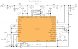
Operating over a 2.8 V to 80 V input range, the IC can produce a 1.3 V to 80 V output, using a single inductor with four-switch synchronous rectification. Fig. 1 shows a voltage stabilizer that provides a regulated 48 V at 5A, even though the input varies from 36 V to 80 V. A single device can deliver up to 250 W, but can achieve a higher output by paralleling multiple circuits.
Operating frequency is selectable between 100 kHz and 400 kHz by placing an appropriate resistor from the RT pin to ground (215 kΩ in Fig. 1) and tying the SYNC pin to GND. You can also synchronize the switching frequency to an external clock using the SYNC pin.
An external feedback resistive divider sets the output voltage. An error amplifier accepts the resultant feedback signal (FBOUT) and compares it with a precision voltage reference (typically1.207V) to control the output voltage, which is:

Where:
RFBOUT1 and RFBOUT2 are shown in Fig. 1 as
392 kΩ and 10 kΩ, respectively.Fig. 1. LT8705 employed as a 48 V stabilizer
The LT8705 employs a proprietary topology and current-mode control architecture for constant frequency operation in buck or boost modes. It employs a current-sensing resistor (RSENSE) in buck or boost modes. Four error amplifiers allow it to regulate or limit the output current (EA1), input current (EA2), input voltage (EA3) and/or output voltage (EA4). In a typical application, the output voltage might be regulated using EA4, while the remaining error amplifiers monitor input or output current.
The LDO33 pin provides 3.3V for external circuitry such as a micro controller or other peripherals. Its maximum load current limit is 17mA. As long as the SHDN pin is high, the LDO33 output is linearly regulated. An undervoltage lockout, monitoring LDO33, disables the switching regulator when LDO33 is below 3.04 V (typical).
Additional features include servo pins to indicate which feedback loops are active, adjustable soft-start, and ±1% reference voltage accuracy over an operating junction temperature range of -40 °C to 125 °C.
POWER SWITCH CONTROL
Fig. 2 is a simplified diagram of the four external power switches connected to the inductor, VIN, VOUT and ground. Fig. 3 shows the regions of operation for the LT8705 as a function of VOUT -VIN or switch duty cycle DC. By properly controlling the power switches there is a seamless transfer from one mode to another.
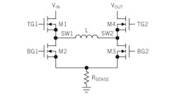
Fig. 2. Simplified diagram of the four NMOS power MOSFET switches.
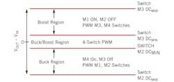
Fig. 3. Buck-boost operating regions vs VOUT – VIN
The four external N-channel power MOSFETs include two for the top switches (M1 and M4, in Fig. 3) and two for the bottom switches (M2 and M3). When VIN is significantly higher than VOUT, the part will run in buck (step-down) mode. In this region M3 is always off and M4 is always on unless reverse current is detected while in Burst Mode® operation or discontinuous mode. Switches M1 and M2 will alternate, behaving like a typical synchronous buck regulator.
As VIN and VOUT get close to each other, the LT8705 operates in buck-boost mode and all four MOSFETs are switching. When VOUT is significantly higher than VIN, the part will run in boost (step-up) mode. In this region M1 is always on and switch M2 is always off. Switches M3and M4 will alternate, behaving like a typical synchronous boost regulator.
The most efficient circuit will use MOSFETs that dissipate the least amount of power. For most buck-boost applications, the M1 and M3 switches have the highest power dissipation where M2 has the lowest, unless the output is shorted. In some cases, it can be helpful to use two or more MOSFETs wired in parallel to reduce power dissipation in each device. However, the additional capacitance resulting by the paralleled MOSFETs can slow switching rates and increase power losses.
MOSFET gate drivers may benefit by adding a 1Ω to 10Ω resistor between NMOS gates and their respective LT8705 gate driver outputs (TG1, BG1, TG2, BG2). Parasitic inductance and capacitance can cause ringing to occur at pins SW1 or SW2 when low capacitance MOSFETs are turned on/off too quickly. Adding gate resistance minimizes ringing, but can slow switching speed. Ringing may be a concern when operating the MOSFETs or the LT8705 near the rated voltage limits.
Ensure that selected MOSFETs can operate with the available gate voltage amplitude, which is 6.35 V, so use logic-level MOSFETs with an RDS(ON) specified at VGS = 4.5 V. With a 25 V maximum input voltage, use MOSFETs rated at 30 V or more. Maximum I2R dissipation in the boost region happens when VIN is minimum. M2’s maximum dissipation occurs at maximum input voltage when the circuit operates in the buck region. For M3 and M4 use MOSFETs with 20 V or higher rating; their highest dissipation occurs in the boost region when input voltage is minimum and output current is maximum.
Low frequency operation increases efficiency by reducing MOSFET switching losses, but requires more inductance and/or capacitance to maintain low output ripple voltage. For high power applications, consider operating the controller at lower frequencies to minimize MOSFET heating from switching losses.
If the die junction temperature reaches approximately a 165°C threshold, the IC goes into thermal shutdown where power switches and internal regulators turn off. The IC re-enables when the die temperature drops by ~5 °C (nominal).
After re-enabling, the IC will start in the switcher off state. Then, the IC initializes, performs a soft-start, and enters normal operation as long as the die temperature remains below its shutdown threshold.
REGULATION
The controller has two constant-current regulation loops, one for the input and one for the output. One sensing resistor monitors the input current by converting it to a voltage that is sensed by the LT8705. The resulting voltage is linearly proportional to the input current. Another sensing resistor monitors the output current and generates a voltage that is linearly proportional to the output current.
The LT8705 buck-boost controller uses inductor current mode control. It measures the peak inductor current in the boost region and the valley of the inductor current waveform in the buck region. The inductor current is sensed across the RSENSE resistor. During any given cycle, the VC pin voltage controls the peak (boost region) or valley (buck region) of the inductor current.
Slope compensation provides stability in constant frequency current mode control architectures. A slope compensation ramp is added to the inductor current in the boost region, and subtracted from inductor current in the buck region. At higher duty cycles, this reduces the maximum inductor current in the boost region, and increases the maximum inductor current in the buck region. It also prevents unwanted sub-harmonic oscillations.
INDUCTOR SELECTION
For high efficiency, select an inductor with low core loss and low DC resistance, which reduces I2R losses. Plus, the inductor must be able to handle the peak inductor current without saturating. To minimize radiated noise, use a toroid, pot core or shielded bobbin inductor.
Input and output capacitors suppress voltage ripple caused by discontinuous current moving into and out of the regulator. Usually, you can use a parallel combination of high capacitance, higher ESR (equivalent series resistance) and low ESR, lower capacitance capacitors. Dry tantalum, special polymer, and ceramic capacitors, as well as OS-CON and POSCAP with low ESR and high ripple current ratings are available. The CIN capacitor network must have low enough ESR and be able to handle the maximum RMS current. Low ESR ceramic capacitors can significantly reduce input ripple voltage and help reduce power loss in the higher ESR (higher capacitance) bulk capacitors. The output capacitance (COUT) reduces the output voltage ripple caused by discontinuities and ripple in the output and load currents.
Place ceramic capacitors near the regulator input and output to suppress high frequency switching spikes. Also, place a ceramic capacitor of at least 1μF. with the maximum VIN operating voltage ratings installed from VIN to GND asl close to the LT 8705 pins as possible. X5R or X7R dielectrics are preferred because they retain their capacitance over wide voltage and temperature ranges.
SCHOTTKY DIODES
The Schottky diodes, D1 and D2, shown in Fig. 1, conduct during the dead time between the conduction of the power MOSFET switches. They prevent the body diodes of synchronous switches M2 and M4 from turning on and storing charge. For example, D2 significantly reduces reverse-recovery current between switch M4 turn-off and switch M3 turn-on, which improves converter efficiency, reduces switch M3 power dissipation and reduces noise in the inductor current sense resistor (RSENSE) when M3 turns on. To be effective, the inductance between the diode and synchronous switch must be minimal, so place them adjacent to each other.
Silicon diodes are recommended for boost diodes DB1 and B2. Make sure that DB1 and DB2 have reverse breakdown voltage ratings higher than VIN(MAX) and VOUT(MAX) and have less than 1mA of reverse leakage at the maximum operating junction temperature. Also, make sure that reverse leakage current at high operating temperatures and voltages do not cause diode thermal runaway.
LOOP COMPENSATION
Several factors affect power supply loop stability, including inductor value, output capacitance, load current, VIN, VOUT and the feedback loop resistor and capacitors connected. The LT8705 uses internal transconductance error amplifiers driving VC to help compensate the control loop. For most applications, a 3.3 nF series capacitor at VC is a good value. The parallel capacitor (from VC pin to GND) is typically 1/10th the value of the series capacitor to filter high frequency noise. A larger VC series capacitor value may be necessary if the output capacitance is reduced. In Fig. 1, the controller’s loop compensation network employs a 56.2 kΩ resistor, plus a 220 pF and 3.3 nF capacitor .
About the Author

Sam Davis
Sam Davis was the editor-in-chief of Power Electronics Technology magazine and website that is now part of Electronic Design. He has 18 years experience in electronic engineering design and management, six years in public relations and 25 years as a trade press editor. He holds a BSEE from Case-Western Reserve University, and did graduate work at the same school and UCLA. Sam was the editor for PCIM, the predecessor to Power Electronics Technology, from 1984 to 2004. His engineering experience includes circuit and system design for Litton Systems, Bunker-Ramo, Rocketdyne, and Clevite Corporation.. Design tasks included analog circuits, display systems, power supplies, underwater ordnance systems, and test systems. He also served as a program manager for a Litton Systems Navy program.
Sam is the author of Computer Data Displays, a book published by Prentice-Hall in the U.S. and Japan in 1969. He is also a recipient of the Jesse Neal Award for trade press editorial excellence, and has one patent for naval ship construction that simplifies electronic system integration.
You can also check out his Power Electronics blog.
Comment About the Article
To join the conversation, and become an exclusive member of Electronic Design, create an account today!

Leaders relevant to this article: