Nano-Packaged Switcher IC Boosts Performance, Cuts Package Size
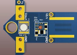
The LMR22007 is the newest member of Texas Instruments’ SIMPLE SWITCHER® family. The brand is almost 25 years old, having been originally born at National Semiconductor and now lives on in the Texas Instruments IC portfolio. Fig. 1 is a mini demo board that illustrates the converter’s size; the board can operate from a computer’s USB port.This IC features high performance and nano-packaging to drive space-constrained and power dense applications.
Related Articles
- 10-A Simple Switcher® Power Module
- SIMPLE SWITCHER Nano Modules And Nano Regulators
- Simple Switchers Go Synchronous
- New Module Family Can Make Any Engineer a Power Supply Designer
- Auto Compensation Enhances Power Supply Designs
- Eight-Channel Configurable 1A Buck DC/DCs for Multi-Rail Systems
- ZVS Buck Regulator Boosts Power In POL Applications
- Innovative Design Shrinks Buck Converter Size, Cuts External Parts Count
- P.C. Board Inductor Shrinks Buck Regulator
- Power Management Basics: Power Supply Characteristics
From the beginning, the SIMPLE SWITCHER concept was intended to make it easier for designers at all skill levels to produce power supplies-and it still does 25 years after it was introduced. And, it is aided by the WEBENCH® online design tool that simplifies and speeds the process.
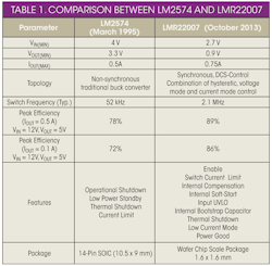
Looking back, I was able to resurrect the LM2574 data sheet, which is dated March 1995. The table compares some of the important characteristics of the LM2574 and the LMR22007. This table reflects the IC design improvements since 1995 as well as the reduction in supply voltages during those years. It also demonstrates the changes made in packaging ICs as well as the power handling capability of smaller size packages. Plus, it indicates the ability to operate switch-mode supplies at MHz switching frequencies. Higher switching frequencies reduce the physical size of LC filters that meet EMI standards and aid in keeping the fundamental frequency and its harmonics out of the AM band. This makes ICs that operate at these switching frequencies more adaptable to automotive applications.
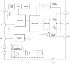
The LMR22007 (Fig. 2) supplies a regulated output voltage by varying the on-time of its internal NMOS switch. During the on-time, the SW pin voltage swings up to approximately VIN, and the inductor current increases with a linear slope. The switch is turned off by the control logic. During the switch off-time, inductor current discharges through the low side device, which forces the SW pin to swing below ground by the voltage drop across the low side device. The regulator loop then adjusts the duty cycle to maintain a constant output voltage.
The IC’s synchronous switched mode power converters are based on DCS-Control™ (Direct Control with Seamless Transition into Power Save Mode). This advanced regulation topology combines the advantages of hysteretic, voltage mode and current mode control, including an AC loop directly associated to the output voltage. This control loop takes output voltage change information and feeds it to a fast comparator. It sets the switching frequency, which is constant for steady state operating conditions, and provides immediate response to dynamic load changes. To get accurate DC load regulation, it uses a voltage feedback loop. The internally compensated regulation network achieves fast and stable operation using low ESR capacitors.
The DCS-Control™ topology supports PWM (Pulse Width Modulation) mode for medium and heavy load conditions and a Power Save Mode for light loads. During PWM, it operates at its nominal switching frequency in continuous conduction mode with a controlled frequency variation depending on the input voltage. If the load current decreases, the converter enters Power Save Mode to sustain high efficiency down to very light loads. In Power Save Mode, the switching frequency decreases linearly with the load current. Since DCS-Control supports both operation modes within one single building block, the transition from PWM to Power Save Mode is seamless without affecting the output voltage.
The simplest way to enable LMR22007operation is to connect the EN pin to VIN, which allows self-start-up when applying an input voltage. You can also connect the EN pin to a voltage source greater than 0.9V to enable operation. Applying a voltage less than 0.4 V puts the IC into a shutdown mode. In shutdown mode the quiescent current drops to typically 300 nA. An internal pull-down resistor of about 400 kΩ keeps EN logic low, if the pin is left floating. The pull-down resistor is disconnected if the pin is held high.
Input Current Limit
The LMR22007 offers a user-adjustable input current limit. Limiting the input current can be useful when the upstream power supply has a tight current budget or when smaller inductors need to be used.
The input current limit can be set over a range of 150 mA to 1000 mA by connecting a resistor from 100k to 15k from the ILIM pin and ground. The higher the value of the RLIM resistor, the lower the average input current limit.
The higher the ripple current in the inductor the more the input current limit will vary with input voltage. However, variation of the input current limit is usually only significant when the inductor ripple current is comparable in magnitude to the current limit to be set.
The LMR22007 uses cycle-by-cycle current limiting to protect the output switches. During each switching cycle, a current limit comparator detects if the low side device current exceeds the low side current limit. If the low side current limit is exceeded the part skips the next on-time pulse until the current falls below the limit. This protects the part from current run-away due to short circuits of the output.
The LMR22007 has a fixed internal soft-start of 3.3 ms (typ). During soft-start, the error amplifier’s reference voltage ramps from 0.0 V to its nominal value of 0.9 V in approximately 3.3 ms. This forces the regulator output to ramp in a controlled fashion, which helps reduce inrush current. Upon soft-start the IC will initially be in diode emulation mode to avoid discharging a pre-biased load.
The LMR22007 has a built in power good (PG) function to indicate whether the output voltage has reached its appropriate level or not. The PG signal can be used for startup sequencing of multiple rails. The PG pin is an open-drain output that requires a pull-up resistor to the appropriate logic voltage (any voltage below 20 V).
Thermal shutdown limits total power dissipation by turning off the internal switches when the IC junction temperature exceeds 155 °C (typ.), and the part is switching in constant conduction mode. After thermal shutdown occurs, hysteresis prevents the part from switching until the junction temperature drops to approximately 130 °C.When the junction temperature falls below 130 °C, the LMR22007 will attempt to soft-start.
External Components
A 2.2µH inductor is recommended to optimize the performance of the LMR22007 for stability and performance. Inductor selection is critical to the performance of the LMR22007. The selection of the inductor affects stability, transient response and efficiency.
The recommended value for the output capacitor is 22 µF. The architecture of the LMR22007 allows the use of tiny ceramic output capacitors with low equivalent series resistance (ESR). These capacitors provide low output voltage ripple and are recommended. To keep its low resistance up to high frequencies and to get narrow capacitance variation with temperature, it's recommended to use X7R or X5R dielectric. The final selection of output capacitor is based upon the desired output ripple and transient response. The LMR22007’s loop compensation is designed for ceramic capacitors. A minimum of 10 µF is required and a maximum value of 200µF is allowed.
For most applications, 10 µF input capacitor will be sufficient and is recommended, though a larger value reduces input current ripple further. The input capacitor buffers the input voltage for transient events and also decouples the converter from the supply. A low ESR multilayer ceramic capacitor (X5R, X7R) is recommended for best filtering and should be placed between VIN and PGND as close as possible to those pins.
PCB Layout Considerations
The performance of any switching converter depends as much upon the layout of the PCB as the component selection. Parasitic inductance can be reduced by keeping the power path components close together and keeping the area of the loops small, on which high currents travel.
1. Minimize area of switched current loops. From an EMI reduction standpoint, it is imperative to minimize the high di/dt paths during PC board layout. The high current loops that do not overlap have high di/dt content that will cause observable high frequency noise on the output pin if the input capacitor CIN is placed at a distance away from the LMR22007. Therefore, place CIN close as possible to the LMR22007 VIN and PGND pins. This will minimize the high di/dt area and reduce radiated EMI. Additionally, grounding for both the input and output capacitor should consist of a localized top side plane that connects to the PGND pin.
2. Have a single point ground. The ground connections for the feedback, and enable components should be routed to the AGND pin of the device. This prevents any switched or load currents from flowing in the analog ground traces. If not properly handled, poor grounding can result in degraded load regulation or erratic output voltage ripple behavior.
3. Minimize trace length to the FB pin. Both feedback resistors, RFBT and RFBB should be located close to the FB pin. Since the FB node is high impedance, maintain the copper area as small as possible. The traces from RFBT, RFBB should be routed away from the body of the LMR22007 to minimize possible noise pickup.
4. Make input and output bus connections as wide as possible. This reduces any voltage drops on the input or output of the converter and maximizes efficiency. To optimize voltage accuracy at the load, ensure that a separate feedback voltage sense trace is made to the load. Doing so will correct for voltage drops and provide optimum output accuracy.
5. Provide adequate device heat-sinking. Use an array of heat-sinking vias to connect the AGND pin to the ground plane on the bottom PCB layer. If the PCB has multiple copper layers, these thermal vias can also be connected to inner layer heat-spreading ground planes. For best results use 0.2 to 0.3mm thermal vias spaced at 1mm. Ensure enough copper area is used for heat-sinking to keep the junction temperature below 125°C.
|
Parameter |
LM2574 (March 1995) |
LMR22007 (October 2013) |
|
VIN(MIN) |
4 V |
2.7 V |
|
VOUT(MIN) |
3.3 V |
0.9 V |
|
IOUT(MAX) |
0.5A |
0.75A |
|
Topology |
Non-synchronous traditional buck converter |
Synchronous, DCS-Control Combination of hysteretic, voltage mode and current mode control |
|
Switch Frequency (Typ.) |
52 kHz |
2.1 MHz |
|
Peak Efficiency (IOUT = 0.5 A) VIN = 12V, VOUT = 5V |
78% |
89% |
|
Peak Efficiency (IOUT = 0.1 A) VIN = 12V, VOUT = 5V |
72% |
86% |
|
Features |
· Operational Shutdown · Low Power Standby · Thermal Shutdown · Current Limit |
· Enable · Switch Current Limit · Internal Compensation · Internal Soft-Start · Input UVLO · Internal Bootstrap Capacitor · Thermal Shutdown · Low Current Mode · Power Good |
|
Package |
14-Pin SOIC (10.5 x 9 mm) |
Wafer Chip Scale Package 1.6 x 1.6 mm |
Table. Comparison between LM2574 and LMR22007
About the Author

Sam Davis
Sam Davis was the editor-in-chief of Power Electronics Technology magazine and website that is now part of Electronic Design. He has 18 years experience in electronic engineering design and management, six years in public relations and 25 years as a trade press editor. He holds a BSEE from Case-Western Reserve University, and did graduate work at the same school and UCLA. Sam was the editor for PCIM, the predecessor to Power Electronics Technology, from 1984 to 2004. His engineering experience includes circuit and system design for Litton Systems, Bunker-Ramo, Rocketdyne, and Clevite Corporation.. Design tasks included analog circuits, display systems, power supplies, underwater ordnance systems, and test systems. He also served as a program manager for a Litton Systems Navy program.
Sam is the author of Computer Data Displays, a book published by Prentice-Hall in the U.S. and Japan in 1969. He is also a recipient of the Jesse Neal Award for trade press editorial excellence, and has one patent for naval ship construction that simplifies electronic system integration.
You can also check out his Power Electronics blog.
Voice Your Opinion!
To join the conversation, and become an exclusive member of Electronic Design, create an account today!

Leaders relevant to this article:


