Using A Supercapacitor To Improve Linear Regulator Performance
Reprinted with permission from Elsevier © 2014
A chapter from the book “Energy Storage Devices for Electronic Systems” describes a design technique that uses a supercapacitor to improve linear regulator performance. This technique is referred to as the Supercapacitor Assisted Low Dropout Regulator (SCALDO) Technique
Related Articles
- MOSFETs Automatically Balance Supercapacitors in High Voltage Commercial Applications
- Small Footprint Low Leakage Current Supercapacitor
- 150mA Supercapacitor Charger with PowerPath Control & Auto Cell Balancing in 9mm²
- Book Review: Devices For Electronic Systems, Rechargeable Batteries And Supercapacitors
- Supercapacitors Enhance LDO Efficiency- Part 2: Implementation Issues
- Supercapacitors Enhance LDO Efficiency- Part 1: Low Noise Linear Power Supplies
6.3.1 Essential Fundamentals
So far our discussion summarizes the fact that in practical electronic systems a combination of different DC-DC converter topologies are used to achieve the overall efficiency, noise minimization, transient response and the packaging issues. If the control circuit consumes only a negligible amount of power the best possible theoretical efficiency of a linear regulator is given by,

Where Vreg and Vp are the regulated output and the input voltages, respectively.
Usually in a linear regulator configuration, most of the energy is dissipated across the pass-element or the series power semiconductor. Introducing a voltage dropper in series with the pass element will make the dissipation across the pass element lower.
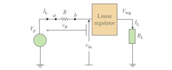
Fig. 6.9 An arrangement of placing a resistor in series with the pass element to make the dissipation lower.
Placing a resistor in series with the pass element as shown in Fig. 6.9 would move some of the energy to the resistor, but this will not improve the overall ETEE.
For this purpose, the ideal voltage dropper element which can be used in the series path is an energy storing element, such as a capacitor or an inductor. If an inductor voltage is used as a voltage dropper, current through the inductor cannot be a constant. A capacitor is the matching candidate as a series dropper element, but in such a case if the capacitance is very small it will block the circuit quickly, stopping the current in a negligible period of time. As discussed in Section 6.1, an extremely large ideal capacitor can be logically used as a lossless dropper in a linear regulator in the series path. The fundamental concept of choosing a supercapacitor as the series dropper element is as follows.
The voltage change (dv) across a very large capacitance C such as a supercapacitor is very small when a finite charge (or discharge) current i(t) flows during a finite time t

A large capacitor, such as a supercapacitor (with negligible ESR value) with a DC voltage can be used as a voltage dropper in the series path, then the effect of the voltage change (dv) due to charging the capacitor for a finite amount of time, can be neglected in terms of the operational principles applicable to that particular circuit. For example, when a large capacitor is connected in series to a circuit for a finite time, the capacitor will not act as a blocking element to that circuit due to charging during that time. Based on this simple principle, using a single supercapacitor or an array of supercapacitors in the series path to store and release the energy, the supercapacitor based efficiency improvement technique suitable for linear regulators was developed (Kularatna and Fernando, 2009,2011).
Register or Sign in below to download the full article in .PDF format, including high resolution graphics and schematics when applicable.
This file type includes high resolution graphics and schematics when applicable.
6.3.2 Basic Concept
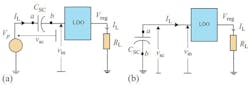
Fig. 6.10 illustrates the concept: a supercapacitor CSC is placed in series with the input of the LDO. Since the series capacitor is large (of the order of farads), it will pass current as it charges for a reasonable period of time. Based on this simple principle, a single supercapacitor can cyclically store and release energy. As per Fig. 6.10 in the first phase of the operation, the supercapacitor is charged from the unregulated power supply. When the value of LDO input voltage, Vin drops to the minimum allowable voltage Vmin_in the operation is switched to the next phase. In this phase, disconnecting the unregulated power supply, the supercapacitor is connected in parallel with the input of the LDO as shown in Fig. 6.10(b), to release the stored energy in the supercapacitor.
Assuming the initial voltage across the supercapacitor (CSC)isVSC(0) after charging for a period t, the instantaneous voltage across the capacitor VSC is given by,

Where IL is the load current entering the capacitor from the unregulated power supply. (We can assume that the load acts as a constant-current sink, and that the bypass current from the LDO to ground can be neglected.)
The unregulated source voltage Vp, equals the sum of the supercapacitor voltage and the LDO input voltage,

The supercapacitor charges until Vin reaches Vmin_in while the voltage across the capacitor reaches Vp - Vmin_in at the end of the charging time. In order to discharge this supercapacitor at the next stage down to Vmin_in, the criterion Vp - Vmin_in be satisfied. This creates the condition Vp > 2Vmin_in.
At the end of the charging cycle, the stored energy can be released as shown in Fig. 6.10(b). Discharging continues until the LDO input voltage drops back to Vmin_in satisfying the following equation,

The circuit draws power from the unregulated input only during half the time of its operating period: during the supercapacitor charging phase, the supercapacitor draws current from the unregulated supply, whereas during the discharging, the supercapacitor delivers power to the LDO keeping the unregulated power supply disconnected from the system.
Considering the charge balance of the supercapacitor during the charge-discharge cycle,

Where tch and tdch are charge time and discharge time, respectively. This gives,

So that the average input current drawn from the unregulated power supply is,

Assuming that the capacitors and switching elements are ideal and neglecting the power consumed by the control circuits, the approximate end-to end efficiency is given by,

The discussion above applies to a practical DC-DC converter such as 12-to-5 V converter, where maximum ETEE possible is 5/12 of 100% which is approximately 42%. In a practical implementation, a supercapacitor can be used with a DC voltage between 6.7 (12-5.3 V) and 5.3 V for case with a commercial LDO chip with a minimum input voltage such as 5.3 V at the regulation. As we see from Eqn (6.11) maximum efficiency achievable is 84%. Practical values of 79-81% were achieved in preliminary proof of concept projects (Kularatna and Fernando, 2009; Kularatna et al.,2010). More discussion on this subject will be found in section 6.6. In general, the practical scenario is, the supercap keeps charging above its average DC voltage within the cycle, in the series mode, and later the supercap releases its charge until it reaches a minimum voltage required for the operation of the LDO, keeping the DC rail disconnected.
Register or Sign in below to download the full article in .PDF format, including high resolution graphics and schematics when applicable.
This file type includes high resolution graphics and schematics when applicable.
6.4 Generalized SCALDO concept
Simple case in the previous discussion requires only one SC and four low-speed switches. However, for general cases of step-down converters, we can extend the basic idea into general case applicable to almost all cases of step-down converters.
6.4.1 Series to parallel SC array
As shown in Fig. 6.11 an array of n ideal series supercapacitors,CSC each, is placed in series with the input of the LDO. This configuration is applicable to a SCALDO regulator, when it satisfies the criterion Vp > 2Vmin_in . Basically, this is the extended version of the single supercapacitor, n=1 case. The number of supercapacitors, n, can be determined using the following formula

As the equivalent capacitance of the series capacitor array is large (in the order of farads), it will pass current as it charges for a reasonable period of time. As per Fig. 6.11 (a) in the first phase of the operation, the series capacitor array is charged until the value of the LDO input voltage, Vin is dropped down to its minimum possible input voltage, Vmin_in .
Assuming the initial voltage across a supercapacitor (CSC)isVSC(0), after charging for a period t, the instantaneous voltage across the capacitor VSC is given by,

Where IL is the load current entering each capacitor from the power supply during the
charging process assuming the ground pin current is negligible.
The voltage across a single capacitor at the end of the charging is,

At the end of this phase, the array of supercapacitors is connected to the input of the LDO as an array of parallel capacitor as shown in Fig. (b) to release the stored energy. This discharging process continues until the LDO input voltage drops back to Vmin_in.
The circuit draws power from the unregulated supply during the supercapacitor charging phase (tch), whereas during the discharge phase (tdch) the supercapacitor delivers power to the LDO keeping the unregulated power supply disconnected from the system.
Considering the charge balance of a single capacitor during charge-discharge cycles,

which gives,

The average input current taken from the unregulated power supply is,

Assuming that the capacitors and switching elements are ideal and neglecting the power consumed by control circuits, approximate ETEE for this configuration is given by,

6.4.2 Parallel to series SC array
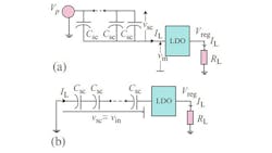
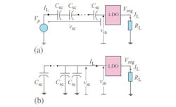
Fig. 6.12 The concept of SCALDO regulator for Vp < 2Vmin_in: (a) Charging n parallel capacitor array minimizing the series element dissipation; (b) Discharging n capacitors series releasing stored energy.
As shown in Fig. 6.12(a) an array of n ideal parallel supercapacitors CSC each, is placed in the input of the LDO. This is applicable to a SCALDO regulator
When Vp > 2Vmin_in .The number of supercapacitors, n, can be determined using the following formula.

As the resultant of the parallel capacitor array is large (in the order of farads), it will pass current as it charges for a reasonable period of time. As per Fig. 6.12(a) in the first phase of the operation, the parallel capacitor array is charged until the value of the LDO input voltage, Vin drops to Vmin_in.
Assuming the initial voltage across a supercapacitor (CSC)isVSC(0), after charging for a period t, the instantaneous voltage across each capacitor VSC is given by,

Where IL/n is the portion of load current entering each capacitor from the power supply during the charging process assuming the ground pin current is negligible. The voltage across a single capacitor at the end of charging is,

As shown in Fig. 6.12(b), in the next phase of operation, using an array of series capacitors, the stored energy is released until the LDO input voltage drops back to Vmin_in.
Considering the charge balance of a single capacitor during charge discharge cycles,

which gives,

Therefore, the average input current drawn from the unregulated power supply is,

Similar to Vp > 2Vmin_in case, under ideal conditions, the approximate ETEE is given by,
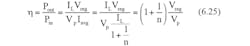
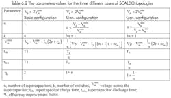
Table 6.2 summarizes the characteristics of the basic configuration which satisfy Vp > 2Vmin_in criterion using a single supercapacitor and the two general configurations which satisfy Vp > 2Vmin_in and Vp < 2Vmin_in the criteria using an array of supercapacitors.

the efficiency improvement factor is a benchmark indication of this technique, and for the two different general cases discussed in Section 6.4, these are (1+ n) and (1+ 1/n) for the two cases of Vp > 2Vmin_in and Vp < 2Vmin_in, respectively.
Register or Sign in below to download the full article in .PDF format, including high resolution graphics and schematics when applicable.
This file type includes high resolution graphics and schematics when applicable.
6.5 Practical Examples
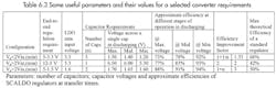
The SCALDO technique can be easily configured for common DC-DC converters such as 12-to-5 V, 5-to-3.3 V, and 5-to-1.5 V and the technique provides efficiency improvement factors of 2, 1.33, and 3 respectively, compared with linear converters with the same input-output combinations (Kularatna and Fernando, 2009;Kularatna et al., 2010,2011a,b,c;Kankanamge and Kularatna, 2012). For example, in a 5-to-1.5 V SCALDO regulator, using thin profile supercapacitors in the range of fractional farads to a few farads, this translates to an approximate ETEE of nearly 90%. Table 6.3 indicates the efficiencies at each transfer stage, assuming that LDO is not abruptly disconnected. This table gives a clear overview of how this novel topology can assist with increasing the ETEE of a linear regulator, with a view to getting the best out of linear-regulator-based DC-DC converters. Practical implementations of these topologies will be discussed in the next chapter.
6.6 SCALDO Implementation Examples
6.6.1 12-to-5 V SCALDO regulator
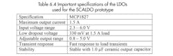
Fig. 6.13 shows the schematic implementation of the 12-to-5 V SCALDO regulator which satisfies the criteria, Vp > 2Vmin_in , in the form of its basic configuration, n = 1. In designing this prototype, an LDO of the type MCP1827 from Microchip Technology Inc., which has the specifications shown in Table 6.4, was used as the main low dropout regulator. For higher-efficiency LDO operation, an approximate LDO input voltage of 0.3 V above the regulated output voltage (5 V) was chosen, so that Vmin_in was maintained at 5.3 V. As the power supply input voltage was around 12 V and the regulated output is 5 V, three supercapacitors of 4 F/2.5 V of the type PC-series from Maxwell Technologies, were connected in series to maintain the required voltage level of the series dropper element. This resulted in 1.33 F/7.5 V resultant capacitor as the series capacitor.
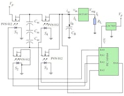
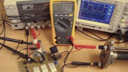
Fig. 6.13 The schematic of the 12-to-5 V SCALDO regulator designed using MCP1827 LDO, 4 F/2.5 V Maxwell Supercapacitors, PVN012 Photovoltaic switches, PIC16F684 microcontroller and LM7805 regulator.
Solid state relays of the type PVN012 from International Rectifier were used as S1, S2, S3, and S4 switches. Switches S1 and S3 control supercapacitor charging, while S2and S4 control the discharge phase. Solid state relays were used in this proof-of concept prototype to avoid complications arising from the body diode of common power MOSFETS. A PIC microcontroller of the type PIC16F684 was used as the controller to drive the photovoltaic switches. An independent 5 V regulator (LM7805) was used to power the microcontroller. The S1,S2, S3, and S4 switches were controlled through the RA0, RA5, RA1, and RA2 port pins of the microcontroller respectively. The LDO input voltage was monitored through the RA4 port pin. The voltage level at this pin is converted to digital format using 10-bit analog to digital converter of the PIC which operates at 4 MHz oscillation frequency. The result is then compared with reference point (digital value of the minimum LDO working voltage, Vmin_in) and the switching between the supercapacitor charge and discharge phases was made accordingly. The microcontroller firmware was developed to drive the switches based on algorithm shown in the flow chart in Fig. 6.14.
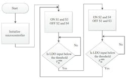
Fig. 6.14 The flowchart of the PIC algorithm.
A switch-over period, tsw was designed to accommodate any transition delays of the PVN012 switches. This creates a short time duration just before the circuit is transferred from the supercapacitor charge mode to the discharge mode. Time duration is set by the PIC micro-controller according to the switch delay. The time duration is determined according to the data sheet of the switch and typically is about 300 ms. Fig. 6.15 shows the delay characteristics of the PVN012 switch.
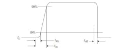
Fig. 6.15 Delay characteristics of PVN012 switches.
To keep the linear regulator powered during the switch transitions, a buffer capacitor (CB) with sufficient capacitance was connected in between the linear regulator input and the ground terminal. In tsw time duration, the buffer capacitor is expected to discharge into the LDO input. The value of the buffer capacitor (CB) can be determined as shown in the Eqn (6.26) using the maximum load current capability of the LDO (Imax_L), switching time delays of a PVN012 switch (tsw) and the minimum possible input voltage at the LDO input (Vmin_in). 1000 mF electrolytic capacitor was chosen as the CB for the 12-to-5 V SCALDO design.

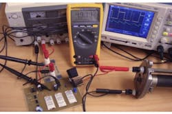
Fig. 6.16 Prototype of 12-to-5 V SCALDO regulator.
