“Quiet” LDO Employs Unique Architecture to Cut Noise and Boost PSRR
Intended for powering noise sensitive applications, Linear Technology has introduced the LT3042, a low dropout (LDO) linear regulator. This LDO uses a unique architecture that minimizes noise effects and optimizes PSRR. To understand the noise performance of this IC, we should first review power source noise characteristics.
Many analog circuits require a low noise power source to prevent unintended output signal errors. The amount of noise a power source produces depends on the device and its output noise bandwidth. The spectral distribution of noise varies with frequency, so you can describe noise voltage (density) by taking the square root of the noise power density, resulting in volts per root Hertz (V/√Hz) In addition, you can evaluate the power source by its integrated output noise by summing all its noise power over the frequency band of interest. This can be expressed as VRMS over a specific frequency band.
This file type includes high resolution graphics and schematics when applicable.
Besides low noise, this power source should reject input power ripple that can affect associated signal output integrity. Power Supply Rejection Ratio or Power Supply Ripple Rejection (PSRR) describes how well a circuit rejects ripple, injected at its input. The ripple can be either from the input supply such as a 50 Hz/60 Hz supply ripple, switching ripple from a DC/DC converter, or ripple due to the sharing of an input supply with other circuits.
For LDOs, PSRR is a function of the regulated output voltage ripple compared to the input voltage ripple over a given frequency range (typically 10 Hz to 1 MHz), expressed in decibels (dB). It can be an important factor when an LDO powers analog circuits because a low PSRR may allow output ripple to affect other circuits.
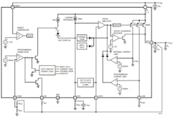
An LDO that reduces noise and increases PSRR is the LT3042 shown in the simplified schematic of Fig. 1.
Rather than a voltage reference used by most traditional linear regulators, the LT3042 uses a current reference that operates with a typical noise current level of 20 pA/√Hz (6 nARMS over a 10 Hz to 100 kHz bandwidth).
The current source is followed by a high performance rail-to-rail voltage buffer, allowing it to be easily paralleled to further reduce noise, increase output current and spread heat on a PCB. Paralleling multiple LT3042s further reduces noise by a factor of √N, where N is the number of parallel circuits.
Key to LT3042 operation is the SET pin that connects to the inverting input of the error amplifier and the regulation set-point (Fig. 1). The SET pin sources a precision 100 μA current that flows through an external resistor connected between SET and GND. The output voltage, VSET, equals the product of ISET and RSET. Output voltage range is from zero to 15 V. The error amplifier’s unity-gain configuration produces a low impedance version of this voltage on its non-inverting input, the OUTS pin, which is tied externally to the OUT pin. Adding a capacitor from SET to GND improves noise, PSRR and transient response at the expense of increased start-up time.
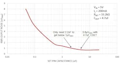
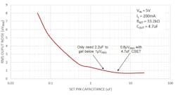
For ultra-low noise applications that require low 1/f noise (at frequencies below 100Hz), the SET pin capacitor of 4.7 μF (maximum recommended 22 µF) reduces noise to 0.8µVRMS. While normally this would significantly increase the regulator’s start-up time, the LT3042 incorporates fast start-up circuitry that increases the SET pin current to about 2 mA during start-up.
The LT3042 eliminates many noise sources present in traditional LDOs. The most critical noise sources for a traditional linear regulator are its voltage reference, error amplifier, and the resistor divider network that sets the output voltage. Traditional linear regulators employ a resistor divider that sets the output voltage gain, but it also increases the reference noise.
In contrast, the LT3042’s unity-gain follower architecture presents no gain from the SET pin to the output. Therefore, if a capacitor bypasses the SET pin resistor, then the output noise is independent of the programmed output voltage. The resultant output noise is then set just by the error amplifier’s noise with a 4.7 μF capacitor connected to the SET pin.
This configuration allows the LT3042 to have loop gain, frequency response and bandwidth independent of the output voltage. As a result, noise, PSRR and transient performance do not change with output voltage. Furthermore, none of the error amp gain is needed to amplify the SET pin voltage to a higher output voltage, and output load regulation is tightly specified in hundreds of microvolts and not as a fixed percentage of the output voltage (as with traditional linear regulators). As a result, the LT3042 characteristics are:
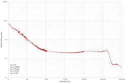
· Spot noise of 2 nV/ √Hz at 10 kHz (Fig. 2)
· Integrated output noise of 0.8 µVRMS from 10 Hz to 100 kHz (Fig. 3)
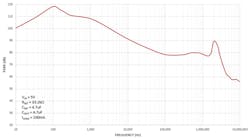
· Low frequency PSRR> 90 dB out to 10 kHz (Fig. 4)
· High frequency PSRR> 75 dB out to 3 MHz
· 200 mA output at a typical 350 mV dropout voltage
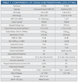
The table compares the characteristics of the LT3042 and a traditional LDO, the LT1962.
Stability
The LT3042 requires an output capacitor for stability. Its high bandwidth (about 1 MHz) requires use of low ESR and ESL ceramic capacitors. Stable operation requires a minimum 4.7 μF output capacitor with an ESR below 50 mΩ and an ESL below 2 nH. To minimize effects of board inductances on the LT3042’s dynamic performance, Kelvin connect the OUTS pin directly to the output capacitor and also Kelvin connect the GND side of the SET pin capacitor (CSET) directly to the GND side of the output capacitor.
In addition, tie the input capacitor’s GND connection as close as possible to the output capacitor’s GND connection. A single 4.7 μF ceramic output capacitor is sufficient; a larger value of output capacitor only marginally improves the performance. This occurs because the regulator bandwidth decreases with increasing output capacitance — hence, there is little to be gained by using larger than the minimum 4.7 μF output capacitor. However, larger values of output capacitance will decrease peak output deviations during a load transient.
This file type includes high resolution graphics and schematics when applicable.
Power Good
In contrast with traditional LDOs, the LT3042 has a Power Good (PG) output (similar to that of a switch-mode power converter). Power Good Feedback pin, PG, goes high if the PGFB (power good feedback) pin increases beyond 300 mV on its rising edge, with 7mV hysteresis on its falling edge. Connecting an external resistor divider between OUT, PGFB and GND programs the power good threshold. As shown in Fig. 1, the voltage divider of external resistors, RPG2 and RPG1 program the power good threshold and also activates the fast start-up circuit. Output voltages below 300 mV disable the programmable power good and fast start-up capabilities.
If you require reverse input protection, tie the anode of a 1N4148 diode to VIN and the cathode to PGFB. Do not drive PGFB more than 0.3 V below GND during normal operation or during a fault condition.
To shut down the LT3042, pull the EN/UV pin low. Operating quiescent current is nominally 2 mA and drops to <1 μA in shutdown. Shutdown turns off the output voltage.
Alternatively, the EN/UV pin can set an input supply undervoltage lockout (UVLO) threshold using a resistor divider between IN, EN/UV and GND. The LT3042 typically turns on when the EN/UV voltage exceeds 1.24 V on its rising edge, with a 170 mV hysteresis on its falling edge. The EN/UV pin can be driven above the input voltage and still maintain proper functionality.
Programmable Current Limit
The ILIM pin’s current limit threshold is 300 mV. Connecting a resistor from ILIM to GND sets the maximum current flowing out of the ILIM pin, which in turn programs the LT3042’s current limit. As shown in Fig. 1, the ILIM pin sources current proportional (1:400) to output current; therefore, it also serves as a current monitoring pin with a 0 V to 300 mV range. For the best accuracy, Kelvin connect this resistor to the LT3042’s GND pin.
In cases where the IN-to-OUT differential is greater than 12 V, the LT3042’s foldback circuitry decreases the internal current limit. As a result, internal current limit may override the externally programmed current limit level to keep the LT3042 within its safe-operating-area (SOA).
Among the LT3042’s other protection features are:
· Short-circuit protection
· Safe operating area protection
· Reverse battery protection
· Reverse current protection
· Thermal shutdown with hysteresis
About the Author

Sam Davis
Sam Davis was the editor-in-chief of Power Electronics Technology magazine and website that is now part of Electronic Design. He has 18 years experience in electronic engineering design and management, six years in public relations and 25 years as a trade press editor. He holds a BSEE from Case-Western Reserve University, and did graduate work at the same school and UCLA. Sam was the editor for PCIM, the predecessor to Power Electronics Technology, from 1984 to 2004. His engineering experience includes circuit and system design for Litton Systems, Bunker-Ramo, Rocketdyne, and Clevite Corporation.. Design tasks included analog circuits, display systems, power supplies, underwater ordnance systems, and test systems. He also served as a program manager for a Litton Systems Navy program.
Sam is the author of Computer Data Displays, a book published by Prentice-Hall in the U.S. and Japan in 1969. He is also a recipient of the Jesse Neal Award for trade press editorial excellence, and has one patent for naval ship construction that simplifies electronic system integration.
You can also check out his Power Electronics blog.
Voice Your Opinion!
To join the conversation, and become an exclusive member of Electronic Design, create an account today!

Leaders relevant to this article:
