42V IC Features Both a 1.5A and a 2.5A Step-Down Regulator Channel
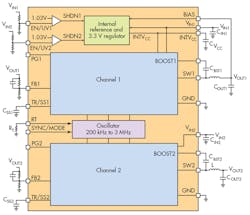
The LT8616 from Linear Technology fills a need for a regulator IC that operates from 3.3V up to a 42V input and provides two separate step-down outputs. Fig. 1 shows a simplified diagram of the LT8616 that contains two regulator channels and associated circuits. One of these circuits is an internal- reference LDO (INTVCC) that supplies 3.4V for the MOSFET drivers and internal bias circuitry. VIN1 powers INTVCC, so it must be present and valid to use either channel. The INTVCC pin must be bypassed to ground with a 1μF ceramic capacitor, which is necessary to supply the high transient currents required by the power MOSFET gate drivers. To improve efficiency, this internal LDO draws current from the BIAS pin when it is at 3.1V or higher. Typically, the BIAS pin is tied to the lowest output or external supply above 3.1V. If the BIAS pin is connected to a supply other than VOUT, bypass it with a local ceramic capacitor. If the BIAS pin is below 3.0V, the internal-reference LDO will consume current from VIN1.
Channel 1 can support a 1.5A load, whereas channel 2 supports a 2.5A load. Channel 1 has a minimum VIN1 requirement of 3.4V, but channel 2 can operate with no minimum VIN2 as long as the minimum VIN1 has been satisfied. VIN1 must be greater than 3.4V for either channel to operate. VIN1 and VIN2 are assumed to be connected to the same input supply. Both channels contain all switches and necessary circuits to minimize the need for external components.
EN/UV1 and EN/UV2 independently disable the associated channel when pulled low and enable it when pulled high. Quiescent current is 6.5μA with both channels enabled. If both EN/UV pins are low, the LT8616 is fully shut down and draws 1.7μA from the input supply. When the EN/UV pins are above 1.03V, the corresponding switching regulators will become active. 1.3μA is supplied by VIN1 to common bias circuits for both channels. The enable pins have accurate 1V thresholds and can be used to program undervoltage lockout.
This file type includes high resolution graphics and schematics when applicable.
An oscillator is common to both channels, which are switched 180 degrees out of phase to prevent interaction between the two channels. Resistor RT sets the frequency from 200 kHz to 3 MHz. Selection of the operating frequency is a trade-off between efficiency, component size, and input voltage range. The advantage of high-frequency operation is that smaller inductor and output capacitor values may be used. The disadvantages are potentially lower efficiency and a smaller input voltage range for full frequency operation.
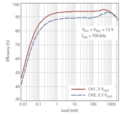
With 12V on both inputs and the operating frequency at 700kHz, the efficiency is shown in Fig. 2. In this case, channel 1 provides 5V out and channel 2 provides 3.3V out.
Internal compensation with peak current-mode topology allows the use of low-inductance value inductors and results in fast transient response and good loop stability. Ground the SYNC/MODE pin for low- ripple Burst Mode operation at low output loads. You can tie to an external clock source for synchronization to an external frequency. Low-ripple Burst Mode operation enables high efficiency down to very low output currents while minimizing output ripple.
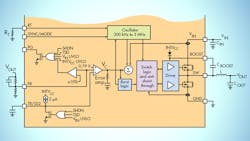
Figure 3 shows one regulator channel of the LT8616. In operation, the oscillator turns on the internal top power switch at the start of each clock cycle. Current in the inductor then increases until the top switch current comparator trips and turns off the top power switch. The peak inductor current at which the top switch turns off is controlled by the voltage at the internal VC node. The error amplifier servos the VC node by comparing the voltage on the FB pin with an internal 0.790V reference. When load current increases, it causes a reduction in the feedback voltage relative to the reference, causing the error amplifier to raise the VC voltage until the average inductor current matches the new load current.
When the top power switch turns off, the synchronous power switch turns on until the next clock cycle begins or the inductor current falls to zero. If overload conditions result in more than the valley current limit flowing through the bottom switch, the next clock cycle will be delayed until current returns to a safe level.
Each channel can independently enter Burst Mode operation to optimize efficiency at light load. Between bursts, all circuitry associated with controlling the output switch is shut down, reducing the channel’s contribution to input supply current. Ground the SYNC/MODE pin for Burst Mode operation or apply a DC voltage above 2.4V to use pulse-skipping mode. If a clock is applied to the SYNC/MODE pin, both channels will synchronize to the external clock frequency and operate in pulse-skipping mode. While in pulse-skipping mode, the oscillator operates continuously and SW transitions are aligned to the clock. During light loads, switch pulses are skipped to regulate the output and the quiescent current per channel will be several hundred μA.
To improve efficiency across all loads, supply current to internal circuitry can be sourced from the BIAS pin when biased at 3.1V or above. Otherwise, the internal circuitry will draw current exclusively from VIN1. The BIAS pin should be connected to the lowest VOUT programmed at 3.3V or above.
The LT8616 allows the designer to program its output voltage ramp rate with the TR/SS pin. Putting an external capacitor on the TR/SS pin enables soft-starting the output to prevent a current surge on the input supply. During the soft-start ramp, the output voltage will proportionally track the TR/SS pin voltage. For output tracking applications, you can drive TR/SS externally from another voltage source. From 0V to 0.790V, the TR/SS voltage will override the internal 0.790V reference input to the error amplifier, thus regulating the FB pin voltage to that of TR/SS pin. When TR/SS is above 0.790V, tracking is disabled and the feedback voltage regulates the internal reference voltage.
PG pins are the open-drain outputs of the internal Power Good comparators. Comparators monitoring the FB pin voltage pull the corresponding PG pin low if the output voltage varies more than ±10% (typical) from the regulation voltage or there is a fault condition.
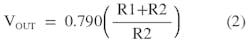
The output voltage is programmed with a resistor divider between the output and the FB pin. Choose the resistor values according to:
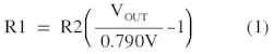
Where:
R1 = Resistor from VOUT to FB in ohms
R2 = Resistor from VOUT to ground in ohms
VOUT = Output voltage
Or
To maintain output voltage accuracy, use 1% resistors. Use large resistor values for the FB resistor divider if you require low input quiescent current and good light-load efficiency. The current flowing in the divider acts as a load current and will increase the no-load input current to the converter. You can connect phase- lead capacitors between FB pins and VOUT nodes, typically 1.5pF to 10pF.
The LT8616 is available in a thermally enhanced 28-lead TSSOP package. Three temperature grades are available, with operation from –40°C to 125°C (junction) for the extended (E) and industrial (I) grades and a high temperature (H) grade of –40°C to 150°C.
This file type includes high resolution graphics and schematics when applicable.
About the Author

Sam Davis
Sam Davis was the editor-in-chief of Power Electronics Technology magazine and website that is now part of Electronic Design. He has 18 years experience in electronic engineering design and management, six years in public relations and 25 years as a trade press editor. He holds a BSEE from Case-Western Reserve University, and did graduate work at the same school and UCLA. Sam was the editor for PCIM, the predecessor to Power Electronics Technology, from 1984 to 2004. His engineering experience includes circuit and system design for Litton Systems, Bunker-Ramo, Rocketdyne, and Clevite Corporation.. Design tasks included analog circuits, display systems, power supplies, underwater ordnance systems, and test systems. He also served as a program manager for a Litton Systems Navy program.
Sam is the author of Computer Data Displays, a book published by Prentice-Hall in the U.S. and Japan in 1969. He is also a recipient of the Jesse Neal Award for trade press editorial excellence, and has one patent for naval ship construction that simplifies electronic system integration.
You can also check out his Power Electronics blog.
Comment About the Article
To join the conversation, and become an exclusive member of Electronic Design, create an account today!

Leaders relevant to this article: