Low-Voltage Logic Inputs Turn 1000Vdc Loads On/Off
The LTM9100 µModule (micromodule) from Linear Technology accepts logic inputs that enable its internal isolated Power Switch Controller to drive an external-power MOSFET/IGBT switching at up to1000Vdc. It uses a galvanic isolation barrier to separate logic inputs from its Power Switch Controller, which can turn high-voltage power sources on and off. In doing so, the isolation barrier protects its low-voltage logic inputs from the neighboring high-voltage Power Switch Controller.
Many computer-based applications employ high voltages that you can control with the LTM9100. One such application is industrial motor drives that may operate from 170Vdc to 680Vdc. Grid-tied solar systems can operate up to 600V or more. Primary power for some modern fighter aircraft is 270Vdc. Li-ion batteries in electric vehicles can reach up to 400V.
In addition, data centers are considering the distribution of high-voltage power to reduce current, I2R cabling losses, and cabling weight. In these types of applications, computer commands can produce logic inputs that enable the LTM9100 to control high voltage power that must be switched on and off with controlled inrush current.
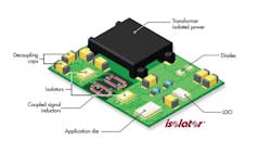
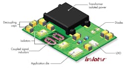
The key to the LTM9100’s power protection is its internal 5kVRMS galvanic isolation barrier that separates the digital input interface from the Power Switch Controller that drives an external N-channel MOSFET or IGBT switch (Fig. 1). The micromodule has an I2C interface that provides access to isolated digital measurements of load current, bus voltage, and temperature, which allows power and energy monitoring of the high voltage bus.
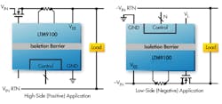
You can configure this isolated power switch controller for use in either high side or low side applications (hence, its Anyside name), as shown in Fig. 2. In addition, it can be used in floating applications.
Adjustable undervoltage and overvoltage lockout thresholds ensure that the load operates only when the input supply is in its valid range. A current-limited circuit breaker protects the supply from overload and short-circuits.
This isolated power switch controller minimizes inrush current by soft-starting the load. It is versatile enough to control inrush current in hot-swappable cards, ac transformers, motor drives, and inductive loads.
An older technique for inrush current control uses negative temperature coefficient (NTC) thermistors or NTC inrush current limiters. These devices start with a high resistance at room temperature before the supply or load is turned on; the high resistance limits the inrush current at turn-on. However, if the circuit is turned off and on quickly there is no inrush current limiting because the resistor hasn’t cooled down enough to regain its high resistance.
Other inrush current control techniques include zero crossing triacs, active power factor control (PFC) circuits, and inductive input filtering with damping. These can be complicated, bulky, and primarily for AC inputs.
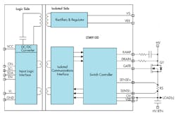
Figure 3 is a simplified diagram of the LTM9100 showing its isolation barrier that divides the micromodule into a logic side and an isolated side. Power for the isolated side employs a fully integrated voltage regulator, including the transformer, so that no external components are required. The logic side contains a full-bridge driver, running at 2MHz, and is ac-coupled to the transformer’s primary. A series dc blocking capacitor prevents transformer saturation due to driver duty cycle imbalance. The transformer scales the primary voltage, which is rectified by a symmetric voltage doubler. This topology reduces common-mode voltage perturbations on the isolated side ground, and eliminates transformer saturation caused by secondary imbalances.
The integrated voltage regulator supplies 10.4V and 5V for the Power Switch Controller. Isolated measurements of load current and two voltage inputs are made by a 10-bit ADC and accessed via the I2C interface. The logic and I2C interface is separated from the Power Switch Controller by the 5kVRMS isolation barrier, which makes the LTM9100 ideal for systems where the Power Switch Controller operates on busses up to 1000VDC. Galvanic isolation is needed for control circuit protection, operator safety, and breaking ground paths.
High-voltage circuits are controlled by encoding signals into pulses and transmitting them across the isolation boundary using coreless transformers formed in the micromodule substrate, as shown in Fig. 4. Uninterrupted communication is guaranteed for common mode transients of 50kV/µs. This system, complete with data refresh, error checking, safe shutdown on fail, and extremely high common mode immunity, is a robust solution for bidirectional signal isolation.
To guarantee a robust isolation barrier, each LTM9100 is production-tested to 6kVRMS. And, it will meet the UL 1577 standard, saving months of certification time for end equipment manufacturers. High distance through-insulation translates to a high ±20kV ESD level across the barrier.
The LTM9100 is ideal for use in networks where grounds can take on different voltages. The isolation barrier blocks high voltage differences and eliminates ground loops and is extremely tolerant of common mode transients between ground planes.
Although its primary application is control of an external N-Channel MOSFET switch, you can also use IGBTs. This may be necessary for voltage applications greater than 250V where traditional MOSFETs with sufficient SOA (safe operating area) and low RDS(ON) may not be available.
IGBTs are readily available with voltage ratings of 600V, 1200V, and higher. Not all IGBTs are suitable, however, only those specified for dc or near dc operation as indicated in their data sheet SOA operating curves. An additional concern is the IGBT’s collector-to-emitter saturation voltage. The Drain pin threshold is 1.77V. In some cases the IGBT saturation voltage, VCE(SAT), may be higher than this, necessitating a voltage divider on the Drain input pin.
The IGBT should be selected with a maximum gate-to-emitter threshold voltage, VGE(TH), corresponding to the minimum LTM9100 GATE power good condition or VS minimum UVLO (under voltage lockout) of 8.5V. The threshold voltage presented in the device data sheet electrical table is often at very low collector currents.
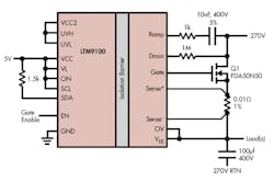
An internal amplifier (A1) connected to the Sense pins monitors the load current through an external sense resistor, RS, providing overcurrent and short-circuit protection. In an overcurrent condition, the current is limited to 50mV/RS by regulating the Gate. If the overcurrent condition remains for more than 530μs, the Gate turns off.
When using a power MOSFET the LTM9100 monitors its Drain and Gate voltages to determine if the MOSFET is fully enhanced. Upon successful turn on of the MOSFET, two Power Good signals are output on the PG and PGIO pins. These pins allow enabling and sequencing of loads. The PGIO pin can also be configured for a general purpose input or output.
Prior to turning on a MOSFET, both the internal gate drive supply voltage VS and VCC2 voltages must exceed their undervoltage lockout thresholds. The MOSFET is held off until all start-up conditions are met.
A 10-bit analog-to-digital converter (ADC) in the Power Switch Controller measures the Sense voltage obtained from amplifier A1. In addition, it measures voltages at the ADIN2 and ADIN pins that are used for auxiliary functions, such as sensing bus voltage or temperature, etc.
The I2C interface enables reading of the ADC data registers. It also allows the host to poll the device and determine if a fault has occurred. You can use the ALERT* pin on the logic input as an interrupt, so the host can respond to a fault in real time. Two three-state pins, ADR0 and ADR1, allow programming of eight possible device addresses. The interface can also be pin configured for a single-wire broadcast mode, sending ADC data and fault status through the SDA pin to the host without clocking the SCL line. This single-wire, one-way communication simplifies system design.
Logic control circuits are powered by an internal LDO that derives 5V from the VS supply. The 5V output is available at the VCC2 pin for driving external circuits (up to 15mA load current). VCC2 is decoupled internally by a 1μF capacitor.
Specified over the −40oC to 105oC temperature range, the LTM9100 is offered in a 22mm x 9mm x 5.16mm BGA package, with 14.6mm of creepage distance between the logic side and the isolated side.

About the Author

Sam Davis
Sam Davis was the editor-in-chief of Power Electronics Technology magazine and website that is now part of Electronic Design. He has 18 years experience in electronic engineering design and management, six years in public relations and 25 years as a trade press editor. He holds a BSEE from Case-Western Reserve University, and did graduate work at the same school and UCLA. Sam was the editor for PCIM, the predecessor to Power Electronics Technology, from 1984 to 2004. His engineering experience includes circuit and system design for Litton Systems, Bunker-Ramo, Rocketdyne, and Clevite Corporation.. Design tasks included analog circuits, display systems, power supplies, underwater ordnance systems, and test systems. He also served as a program manager for a Litton Systems Navy program.
Sam is the author of Computer Data Displays, a book published by Prentice-Hall in the U.S. and Japan in 1969. He is also a recipient of the Jesse Neal Award for trade press editorial excellence, and has one patent for naval ship construction that simplifies electronic system integration.
You can also check out his Power Electronics blog.
Comment About the Article
To join the conversation, and become an exclusive member of Electronic Design, create an account today!

Leaders relevant to this article: