Members can download this article in PDF format.
High efficiency and high power density are critical characteristics when designing power supplies for today’s products. To achieve these goals, developers are turning to gallium nitride (GaN), a wide-bandgap semiconductor technology that achieves high switching frequencies. Compared to competing power semiconductor technologies, GaN minimizes the size of required passive components while simultaneously lowering gate-drive and reverse-recovery losses.
Sponsored Resources
- Take the TOLL Road to More Robust GaN Designs
- Simplify GaN Designs with New Integrated TOLL-packaged GaN Power Stage
- LMG3650EVM-114
In addition, semiconductor manufacturers are packaging their GaN devices in highly integrated industry-standard footprints that shrink printed-circuit-board (PCB) real-estate requirements while streamlining supply chains.
GaN Applications
In the 650-V, AC-DC-conversion space, the transformer outline leadless (TOLL) package is an effective choice for power-supply designs. Devices in this package can incorporate GaN field-effect transistors (FETs) as well as gate drivers and overcurrent, overtemperature, and short-circuit protection circuitry to maximize efficiency and reliability. These devices can operate in totem-pole power-factor-correction (PFC), inductor-capacitor, phase-shifted full bridge, and dual-active-bridge circuit topologies.
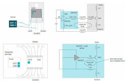
Figure 1 illustrates the advantages of the integrated gate-driver circuitry. Figure 1a shows a separate gate driver and GaN switch. The equivalent circuit on the right reveals the many parasitic elements in the gate hold-off loop, including the driver output inductance (Ldrv_out), the PCB inductances (Lg_pcb), and the power-device gate inductance (Lg_gan). Figure 1b shows the integrated device on the left, with the circuit model (right) showing the parasitics reduced to a negligible level.
TOLL devices with integrated drivers and protection circuitry can serve a variety of applications, including the power-supply units (PSUs) used in hyperscale-computing data centers, where they can convert AC power into a DC bus. Increasing power density is critical in such applications, because equipment power requirements continue increasing while the PSU form factor remains the same.
TOLL devices can serve in both the PFC and DC-DC-converter stages of a PSU. Texas Instruments says its GaN TOLL devices are able to achieve greater than 99% efficiency in the PFC stage and better than 98% efficiency in the DC-DC stage.
Other applications can make use of TOLL GaN devices, too, including large-screen televisions and electric-vehicle (EV) onboard chargers. For televisions, the integrated TOLL GaN devices let designers fit power-supply circuitry, including passive components, within a thin form factor while increasing power density. For EVs, TOLL devices enable onboard charging circuitry to achieve high efficiencies while fitting within the vehicle chassis. For both, the TOLL devices can implement both the PFC and DC-DC stages.
Yet another application is the bidirectional photovoltaic inverter. Operating in one direction, it can invert a solar panel’s DC output to the AC grid voltage, and while operating in the other direction, it’s able to charge backup batteries using power from the AC grid. As shown in Figure 2, TOLL devices can serve in both the totem-pole PFC/inverter stage and in the bidirectional DC-DC converter stage.
TOLL Device Details
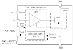
One device suitable for such applications is TI’s LMG3650R035 650-V GaN FET, which offers an on-resistance RDS(on) of 35 mΩ and a maximum drain current of 20 A. To minimize bill-of-materials (BOM) count and PCB real estate, the device, which comes in a TOLL package measuring 9.8 × 11.6 mm, incorporates gate-driver circuitry and advanced protection functions (Fig. 3).
The integrated gate driver supports adjustable gate-drive strength to allow for the independent control of turn-on and turn-off slew rates. Turn-on rates range from 10 to 100 V/ns and turn-off rates extend from 10 V/ns to a maximum level based on the load-current magnitude. The independent adjustments can help optimize switching performance while minimizing electromagnetic interference (EMI).
The device determines the programmed slew rates on startup by sensing external resistor-capacitor networks connected to its drive-strength selection pin. After startup, that pin takes on the role of fault monitoring.
The gate driver also integrates an undervoltage lockout (UVLO) feature and overvoltage and overtemperature protection capability. On top of that, it includes, cycle-by-cycle, an overcurrent protection (OCP) function and a latched short-circuit protection (SCP) function that responds within 300 ns. The device can withstand a 720-V surge while switching.
Versions of the device are available with a zero-voltage detection (ZVD) feature, a zero-current detection (ZCD) feature, or a 5-V low-drop-out (LDO) regulator output that can power an external isolator. The different versions assign ground, the 5-V output, the ZVD signal, or the ZCD signal to the pin shown on the lower left of the Figure 3 block diagram.
Evaluation Module
To help you get started on designs based on the LMG3650R035, TI offers the LMG3650EVM-114 evaluation module, a daughtercard that can be part of a larger custom-designed system or paired with a TI GaN motherboard. Available motherboards include the LMG342X-BB-EVM, which is a DC-DC buck-boost converter that can support up to 4 kW, and the PFC23338EVM-107, an AC-DC totem-pole PFC stage that can support up to 3.6 kW.
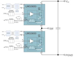
The LMG3650EVM-114 card itself includes two LMG3650R035 GaN ICs in a half-bridge configuration, two digital isolators for the GaN IC fault signals, and isolated bias and bootstrap supplies. The card also incorporates two isolated gate drivers to enable layout compatibility with discrete GaN devices in TOLL packages (Fig. 4).
For testing designs based on the card, TI recommends using a 520-V DC voltage supply, a 12-V at 1.5-A DC bias source, a function generator that can produce 0- to 5-V square waves with adjustable duty cycles, a 1-GHz oscilloscope, a DC multimeter, and a DC load capable of operation at up to 650 V or 20 A.
Conclusion
GaN technology excels at power conversion in applications ranging from large-screen televisions to photovoltaic renewable-energy systems. Incorporating GaN FETs with gate drivers and protection circuitry in TOLL packages helps boost reliability and power density. In addition to a portfolio of GaN products, TI offers an evaluation module that helps you get started on designs based on TOLL products.
Sponsored Resources
- Take the TOLL Road to More Robust GaN Designs
- Simplify GaN Designs with New Integrated TOLL-packaged GaN Power Stage
- LMG3650EVM-114


