Designing a Chip with Open-Source Tools: The Development of Silicluster
What you’ll learn:
- Open-source tools and multi-project wafer (MPW) shuttles democratize chip design for low cost.
- Small circuits, both analog and digital, are accommodated by embedding them as “tiles” or “clusters” into larger chips like “Silicluster” for lower-cost prototying and more efficient debugging/validation.
- How the Silicluster’s ADC and DAC components were designed.
In the world of semiconductor design, the challenges of learning to design chips from scratch are often underestimated. The barriers, both in terms of tools and knowledge, can be overwhelming. However, with the rise of open-source software and hardware initiatives, a new opportunity has emerged for those who wish to take on this challenge.
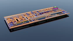
This article details the process of designing Silicluster, a chip designed using open-source tools, with a focus on accessibility and affordability (Fig. 1).
The Beginning of Chip Design
The journey into chip design began unexpectedly. Since childhood, there was always a fascination with how things worked, but it was never imagined that this curiosity would transform into a passion for electronics. The academic path led to studying a Bachelor's in Electronics Engineering, a Master's in Electronic Design, and ultimately a Ph.D. in the same field.
However, it was later when it became evident that the high costs and barriers to access traditional chip design tools were a challenge. In many Mexican institutions, there’s a lack of access to high-end tools due to the prohibitive costs of their licenses.
This realization led to the exploration of open-source tools, which promised to reduce the barriers to semiconductor design. It resulted in the creation of Silicluster, a chip designed with the goal of being affordable and accessible for students, educators, and small businesses alike.
Installation and Learning the Tools
The first obstacle faced in this journey was the installation of the necessary tools. Unlike traditional commercial EDA tools, which have official support and documentation, open-source tools are more of a "do-it-yourself" experience. This was the first interaction with tools like OpenLane for RTL-to-GDS flows and Xschem for schematic capture. While there’s no official support structure, the community and the available documentation helped to get started.
>>Download the PDF of this article

One of the biggest challenges was navigating the complexities of the installation process. Each tool required different dependencies, and even after installation, there was a learning curve to understand how to effectively use them. The reward was worth it, though. Tools like Magic and Netgen, and OpenLane, made it possible to design and manufacture a custom chip for a fraction of the cost of traditional solutions.
The learning process took time, but the collaborative nature of the community made it a more rewarding experience. Today, these tools can be installed with relative ease, and the process has become much smoother thanks to shared knowledge and community efforts.
Design Choice: Silicluster
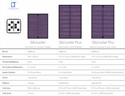
When it came time to choose what chip to design, the goal was to create something that could serve as a foundation for a variety of projects. The idea was to design a chip that could house multiple small modules (up to 256 independent circuits) and be flexible enough to handle both digital and analog signals. This led to the development of Silicluster.
The goal of the chip is to provide a low-cost platform that lets multiple users share manufacturing costs while enabling independent projects. It’s based on a multiplexing architecture, where each project (ASIC or multiplexer) is connected via secondary multiplexers, and the final selection is made by a central multiplexer. This architecture allows for the integration of up to 16 individual blocks, optimizing space usage on the chip.
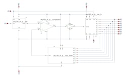
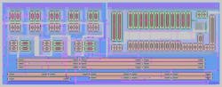
A key part of the design is the 8-bit successive approximation register (SAR) ADC, responsible for converting analog signals to digital (Fig. 2).
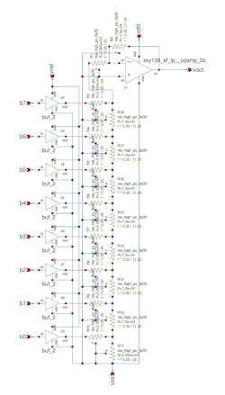
This is complemented with an 8-bit DAC to ensure compatibility between the chip’s digital and analog components (Fig. 3).
The ability to integrate both analog and digital circuits into a single design was one of the most appealing features of Silicluster. It opens up many possibilities for users who wish to build complex systems without the need for separate chips for each function.
The Technology Behind Silicluster
Silicluster was designed using the 130-nm technology from SkyWater, an affordable and powerful option for open-source semiconductor projects. This technology, combined with open-source tools, led to a drastic reduction in the costs associated with chip design and fabrication.
An important aspect to mention is the intermediary in this process: Efabless, the company that facilitates the connection between the designer and the fabrication facility. Through Efabless, it was possible to leverage the available manufacturing infrastructure without the high costs of traditional methods. This collaboration was essential in bringing Silicluster and other projects to life.
Learning Circuit Design
The design of Silicluster involved learning both the fundamental principles of circuit design as well as the specific details required to build a chip that can handle both digital and analog signals. To begin, classic books and online resources were consulted, such as CMOS Analog Circuit Design by Allen and Holberg, to understand the complexities of analog circuits.
At the same time, tutorials and documentation on digital logic design were reviewed, focusing on the interaction between the different components of the circuit. One key takeaway was the importance of making each part of the circuit as efficient as possible.
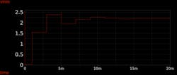
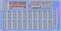
Designing an ADC with reasonable resolution (Fig. 4) that fit within the strict area constraints of the chip (Figs. 5 and 6) while maintaining low power consumption was a challenge that required careful consideration.
The Design Flow: Schematic, Simulation, Layout
After gaining a solid understanding of the circuit requirements, it was time to move on to the design flow. The first step was schematic capture using Xschem. Creating the schematic was both a rewarding and frustrating experience, as numerous decisions had to made regarding the configuration of each component.
After completing the schematic, simulation was done using ngspice to verify that the circuit would function as expected, as shown for the DAC in Figure 7. Simulation helped identify problems such as signal-integrity issues or incorrect configurations that could affect the chip's functionality.

With the schematic validated through simulation, the next phase was the layout. This was particularly challenging, as it required fitting the design into a very small chip area. Space constraints, while exciting in terms of innovation, also created bottlenecks in the design.
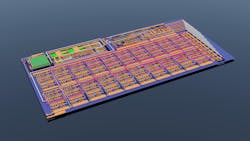
Each component had to be placed, not only correctly connected, but also arranged in a way that minimized interference and maximized performance. This part of the design process required many iterations, as each layout decision affected the subsequent steps (Figs. 8 and 9).

Once the layout was complete, tools such as Magic and OpenLane were used for the final steps: DRC (Design Rule Check), LVS (Layout vs. Schematic), and GDSII generation. Each step of this process required careful attention to ensure the final design could be fabricated without errors.
The most difficult part of the design flow was adjusting everything within the chip's limited area. The constant back and forth between optimizing the design for space, power consumption, and functionality was exhausting, but ultimately necessary, to ensure the chip would function in real-world conditions.
Lessons Learned and Areas for Improvement
Designing Silicluster was a complex but incredibly rewarding process. One of the most important lessons learned was the value of iteration and careful planning. In hindsight, more time could have been spent in the early stages of the design refining the architecture to better fit the layout constraints. This would have saved significant time later in the process, as there were several instances of reworking the design to adapt to the available space.
Another learning experience was that working with open-source tools requires patience and creativity. Many times, the community was consulted for support, whether through forums, issues on GitHub, or reading extensive documentation. The process of making the tools work smoothly taught the value of persistence and collaboration.
What’s Next?
Looking forward, the plan is to continue refining Silicluster and integrate new features into the design. The aim is to improve the chip's energy efficiency and perhaps explore more advanced manufacturing techniques, such as using newer processes or integrating more complex analog-to-digital conversion mechanisms. Moreover, the chip should be more accessible by providing a comprehensive guide for others to design their own chips using the tools learned.
There are other ideas for future projects, including the development of a new type of low-power microcontroller chip aimed at IoT applications. This would build on the lessons learned from Silicluster, but with a more specific focus on certain markets.
Final Thoughts: Would It Be Recommended?
For those with experience in designing digital or analog circuits, trying to design a chip using open-source tools is definitely recommended. The process may seem daunting at first, but the learning experience is invaluable. It’s an excellent way to expand knowledge and gain hands-on experience in semiconductor design.
For beginners, it’s suggested to start with simpler projects before tackling something as complex as Silicluster. But regardless of experience level, the tools and resources available today make chip design more accessible than ever.
>>Download the PDF of this article
About the Author

Uriel Jaramillo Toral
Chip Design Engineer
Uriel Jaramillo Toral, originally from Aguascalientes, Mexico, holds a Bachelor's degree in Electronics Engineering from the Instituto Tecnológico de Aguascalientes (ITA) of TecNM, a Master's degree in Electronic Design, and is currently in the second year of his Ph.D. in CINVESTAV Guadalajara.
His technical background began in Mechatronics at CBTis 168, a technical preparatory school, and he has worked at companies such as Intel and Circuify. Additionally, he completed a 4.5-month academic exchange at the University of Toyohashi, Japan, where he learned about microchip manufacturing. He’s the creator of Silicluster, a chip designed with open-source tools aimed at democratizing access to microchip manufacturing in Mexico.
Comment About the Article
To join the conversation, and become an exclusive member of Electronic Design, create an account today!

Leaders relevant to this article: