The Crystal-Clear Truth About Critical Transconductance
What you'll learn:
- What is a crystal oscillator's impedance?
- A look at the Pierce oscillator topology.
- How to generate negative resistance.
- An alternative approach to determining a crystal oscillator's impedance that offers deeper insight.

Crystal oscillators are essential for precise timing in electronic systems, and most engineers are familiar with their basic principles. Formulas for critical and optimum transconductance are widely used in design, yet their origins often remain opaque.
This article aims to uncover that reasoning, starting from fundamental concepts such as the crystal’s impedance and the Pierce oscillator topology, encompassing oscillator feedback strategies, and proceeding through the derivations step by step. It will demonstrate how these formulas emerge from circuit analysis, allowing the reader to not only understand the formulas, but also know exactly where they come from and why they matter.
Setting the Frequency
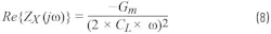
A crystal is a small piece of quartz that exploits the piezoelectric effect: An applied electric field induces mechanical vibration, and mechanical stress generates an electric response. It can be modeled electrically as seen in Figure 1.
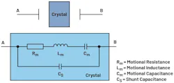
The crystal itself can exhibit series resonance at the frequency:
It also exhibits antiresonance (when in parallel mode) at the frequency:
When an extra capacitor CL is added in parallel with the crystal, the crystal is loaded, and the oscillating frequency becomes:
Typically, Cm « CS, which means the series and parallel resonance frequencies (fS and fP) are very close. Interestingly, the loaded oscillation frequency always falls between fS and fP.
A widely used topology for crystal oscillators is the Pierce configuration (Fig. 2).
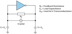
The resistor RF biases the inverter into its linear region, setting the DC operating point without significantly affecting the AC loop behavior. For AC analysis, its influence is negligible and will be omitted. Throughout this article, the inverter is modeled as an ideal transconductance (Gm).
Oscillator Families: Positive Feedback vs. Negative Resistance
Harmonic oscillators fall into two main categories: positive-feedback oscillators and negative-resistance oscillators.
>>Download the PDF of this article

Positive-feedback oscillators operate by feeding a portion of the output signal back to the input with the correct amplitude and phase to satisfy the Barkhausen stability criterion:

where A is the gain and B is the feedback transfer function. This approach is typically used when the gain and feedback paths are explicitly defined, as in Wien bridge or ring oscillators.
Negative-resistance oscillators, however, aim to cancel out the resistive (lossy) elements in the circuit, allowing energy to transfer freely between reactive components. The condition for oscillation becomes:
This perspective is more intuitive when a resonator is present, such as an LC tank or a crystal. Common examples include Hartley, Colpitts, and Clapp oscillators.
Though conceptually different and relying on distinct analytical viewpoints, both approaches describe the same physical phenomenon.
Why Critical Gm Matters in Crystal Oscillators
Among the key design parameters in crystal oscillator circuits, the transconductance plays a central role. If Gm is too low, the oscillator simply won’t start — a failure that can be both subtle and frustrating. To ensure a reliable startup, Gm must exceed a threshold known as the critical Gm.
The Thumb Rule Trap
A simplified expression sometimes encountered for estimating critical transconductance is:
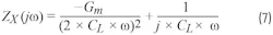
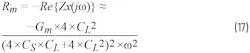
This approximation loosely stems from the Barkhausen criterion and resonance behavior. At series resonance, the crystal’s impedance simplifies to Z ≈ Rm (neglecting CS), and the loop gain is approximated as A × B = Gm × Rm > 1. However, this model doesn’t reflect the Pierce oscillator topology and produces results that are not only incorrect, but also directly contrary to the intended behavior. As shown later, an increase in Rm actually demands a higher Gm.
Generating a Negative Resistance
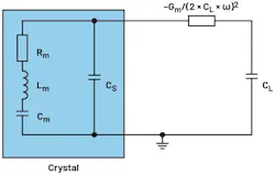
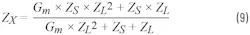
As noted earlier, because the circuit includes a resonator, the negative-resistance approach is the more suitable method of analysis. A simple way to create a negative resistance is to look at the input impedance of the topology (Fig. 3).
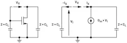
Calculate the dynamic impedance seen at VX to prove it’s of the form:
which created a negative resistance equal to:
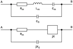
The AC circuit seen by the crystal is equivalent to the circuit in Figure 4.
Using basic impedance transformation, derive:
The real part of that impedance can be shown as:
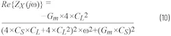
To offset the resistive losses, the negative resistance must equal the motional resistance:
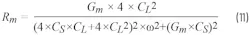
which leads to the following quadratic equation:
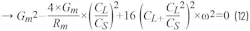
Calculating the discriminant ∆ will allow us to determine if a real solution (∈ ℝ) exists.
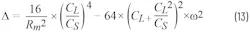
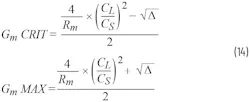
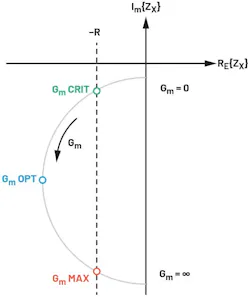
If the discriminant Δ is negative, the system has no real solutions. If Δ is positive, two values of Gm satisfy the equation, and oscillation is possible for any value in between. The lower bound is known as the critical transconductance Gm_CRIT, which is the minimum required for startup. The upper bound is the maximum transconductance Gm_MAX, beyond which stable oscillation can’t be sustained. Exact values can be determined using a numerical solver:
Solving the condition:
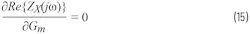
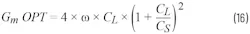
can determine the optimum transconductance, which corresponds to the point where the negative real part of the impedance seen by the crystal is maximized. This yields the expression:
As Gm increases from 0 toward +∞, the impedance seen by the crystal evolves in the complex plane. This progression illustrates the transition from critical Gm, through optimum Gm, up to maximum Gm. Outside this range, the losses can’t be compensated, and the system can’t sustain oscillations (Fig. 6).
The value of interest is usually Gm_CRIT. Assuming Gm × C2 « 4 × (C × C + C2)2 × ω2, then the impedance Z can be approximated as:
This simplification is sometimes referred to as the small Gm approximation. The physical intuition is that Rm is small (as crystals have very high-quality factors, ranging from 10,000 to 100,000), and thus the associated losses are minimal. Consequently, the contribution of the negative impedance circuit (Gm) should be minimal. Under this assumption, the critical Gm can be expressed in a more compact form:

A Detour that Delivers Insight
The previous method treats the crystal as a general impedance, without distinguishing between its resistive and reactive components. An alternative approach exists whereby, while slightly longer to derive, offers deeper insight and practical benefits.
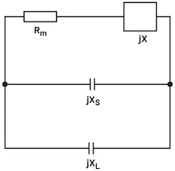
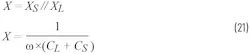
To begin, simplify the motional branch of the crystal by grouping its inductive and capacitive elements into a single reactance term, X. For consistency in notation, the shunt capacitance reactance is defined as jXS, with XS = −1/(CS × ω) (Fig. 7).
The impedance of the crystal (between A and B) can be written as:
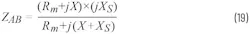
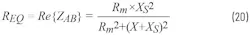
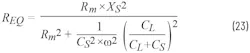
The effective resistance between nodes A and B corresponds to the real part of the impedance seen across those points:
With the crystal connected to the load capacitor, the circuit can now be drawn as shown in Figure 8.
At resonance, the reactive components cancel each other out, hence:
Inserting this result into the previous REQ equation gives us:
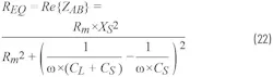
which can be simplified as:
If the assumption:
is true, the crystal’s equivalent resistance seen by the amplifier can be approximated as:
This formula provides a useful link between the crystal’s internal power dissipation, its motional resistance Rm, and the capacitance ratio CS/CL. Crystals have a maximum allowable power dissipation, beyond which long-term reliability may be compromised. The dissipated rms power can now be estimated as Prms = REQ × I ms2 to verify that the oscillator operates within safe drive levels.
Unfortunately, the term REQ is often referred to as equivalent series resistance (ESR) and used inconsistently in oscillator design. In some contexts, ESR refers to the effective resistance seen by the amplifier (what’s been called REQ). In others, it denotes the motional resistance (electrical series resistance), which represents the intrinsic losses within the crystal itself (what’s been called Rm).
To add to the confusion, some vendors label Rm as ESR, while certain documents use ESR to describe Rm in the context of critical Gm calculations. Typically, CS is much smaller than CL, making Rm and REQ numerically close. This may explain why the distinction often goes unnoticed.
Hopefully, this clarification helps the reader differentiate between the two and understand which value is appropriate in each context: calculating startup conditions, resonant frequency, or estimating drive level.
Returning to the equivalent circuit, the oscillator can now be represented as shown in Figure 9.
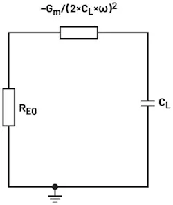
Once again, to sustain oscillation, the negative resistance presented by the amplifier must cancel out the equivalent resistance seen from the crystal:
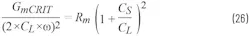
Rearranging Equation 26 gives the same expression previously derived for the critical transconductance:

The Power of Four
Ultimately, the critical Gm represents the precise mathematical threshold required for sustained oscillation. It ensures that the energy lost in the crystal is exactly compensated by the amplifier.
However, to guarantee a reliable startup under real-world conditions, designers typically provide excess Gm. This accounts for variations in Rm, drive-level dependencies, and startup dynamics. A safety factor of 4 is commonly applied in practice to ensure robust performance across temperature, aging, and process variations.
Conclusion
This article demonstrates why critical Gm is essential for crystal oscillator startup and stability. We explored the dependencies with Rm, CS, and CL, highlighted the common pitfall of relying solely on 1/Rm, and presented two complementary approaches to solving the problem. Each method offers unique insights: one provides a complete view of the operating range, while the other reveals a key relationship with drive level.
Understanding these principles equips designers to move beyond rules of thumb and apply precise calculations that ensure reliable startup and robust performance under real-world conditions.
References
Frerking, Marvin E. Crystal Oscillator Design and Temperature Compensation. Litton Educational Publishing, Inc., 1978.
Razavi, Behzad. “The Crystal Oscillator.” IEEE Solid-State Circuits Magazine, Vol. 9, June 2017.
Vittoz, Eric, Marc Degrauwe, and Serge Bitz “High-Performance Crystal Oscillator Circuits: Theory and Application.” IEEE Journal of Solid-State Circuits, Vol. 23, June 1988.
>>Download the PDF of this article
About the Author
Jerome Rollet
Staff Analog Design Engineer, Analog Devices Inc.
Jerome Rollet is a staff analog design engineer in the Data Center and Energy Group at Analog Devices. Prior to joining ADI in 2014, he was a member of technical staff at Maxim Integrated. Jerome has 17 years of expertise in power management and mixed-signal circuit design across consumer, industrial, and automotive applications.
He holds a Master of Science in electronic engineering from the Grenoble Institute of Technology and a Master of Research in microelectronics and nanoelectronics from Grenoble Alpes University.
Comment About the Article
To join the conversation, and become an exclusive member of Electronic Design, create an account today!

Leaders relevant to this article: