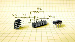
Amplifier Techniques that Lead to Precision Performance
What you’ll learn:
- Modern precision amplifiers achieve lower cost through CMOS-based techniques like e-trim and zero-drift calibration, reducing the need for laser trimming in many cases, and shortening test time.
- Precision devices can lower total system cost by minimizing calibration, design complexity, and error sources compared to general-purpose amplifiers.
For many years, precision amplifiers have carried a cost premium for high performance. However, new amplifiers are achieving increasingly better precision at reduced cost. This article will explain how modern technologies facilitate an excellent cost/performance tradeoff, as well as the typical limitations of these technologies.
What is Precision Analog and When Does It Matter?
Precision analog generally refers to the DC accuracy of the device. For amplifiers, this means a low input offset voltage (VOS), low offset temperature drift (dVOS/dT), and low input bias current (IB). All of these parameters will introduce an unwanted shift in the DC transfer function of the device. The VOS and other DC error sources can be modeled as a DC voltage source in series with the operational amplifier’s (op amp) noninverting input. This error source will often directly add to the input signal.
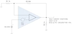
For amplifiers in high gain, the input offset can introduce very large errors and may even be comparable to the input signal amplitude. Figure 1 shows an example of an application in high gain with an amplifier that has a relatively high VOS. In this case, the VOS is 1 mV and the input signal is only 20 mV, so the error is 5%.
In many practical applications, such as bridge sensors or thermocouples, the sensor output is a millivolt-level DC signal. It is important to use precision amplifiers in these cases to minimize errors. On the other hand, applications like audio are more focused on the amplifier’s AC characteristics, such as distortion and noise. These applications are generally AC-coupled, so the DC offset is effectively blocked by the coupling capacitor. When choosing an amplifier, first decide if the application is targeted more toward DC precision or AC performance.
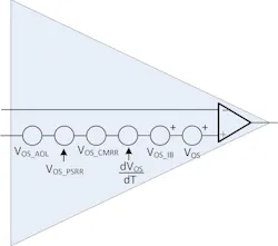
Besides VOS, dVOS/dT, and IB, secondary effects will bring on additional offset sources. For example, open-loop gain (AOL), power-supply rejection ratio (PSRR), and common-mode rejection ratio (CMRR) can all generate additional VOS. The application note “Op Amp Offset Voltage and Bias Current Limitations” covers the mathematical details on these sources. While the secondary errors will be less significant than VOS, in some cases they can be significant (Fig. 2).
What is “e-trim” Technology?
VOS is caused by a mismatch on the input differential transistor pair inside the op amp. If the transistors were perfectly matched, the amplifier would not have any offset. However, because of process variations, photolithography limitations, and package-induced stress, the input transistors don’t match.
One way to correct for the VOS error is to trim the device by adjusting the resistors connected on the source of each input transistor (Ros1 and Ros2 in Fig. 3). The resistors develop an adjustable voltage that can cancel the offset. Years ago, designers adjusted VOS with an external potentiometer on the applications circuit. Later, manufacturers used laser-trimming and e-trim technologies to reduce VOS.
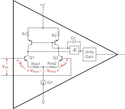
Laser trimming refers to a process where manufacturers measure VOS and adjust it during the manufacturing test by using a laser beam to cut away resistor material. Another method for reducing offset is Texas Instruments’ e-trim technology. This procedure measures offset during the manufacturing test and sends a digital code to blow fuses, shorting or opening them in parallel with the resistors.
For CMOS devices, a second set of resistors needs trimming to correct for temperature drift error (R1 and R2 in Fig. 3). In the case of bipolar devices, one set of resistors trims both VOS and VOS temperature drift.
What is Zero Drift?
The term zero drift describes amplifiers that use an internal calibration method to reduce input offset voltage and offset drift. Since many parameters are defined as a shift in VOS, the zero-drift method will improve these specifications because the shift will be calibrated internally. The CMRR, PSRR, and AOL on zero-drift devices are all quite good since these specifications are based on offset.
Other methods for correcting VOS, such as e-trim technology, will not inherently improve CMRR, PSRR and AOL as is the case with zero drift. Zero-drift calibration also minimizes low-frequency 1/f noise for amplifiers.
VOS and VOS drift of zero-drift devices will generally be better than laser-trimmed or e-trim devices, which might suggest that zero-drift amplifiers are generally the best choice for applications requiring good DC accuracy. But that’s not always true.
The main limitation of zero-drift devices is that they use internal switches on the input pins, which generate bias current transients (Fig. 4). These transients can convert into VOS for large source or feedback impedances. The transients also contain noise tones at the chopper frequency and harmonics of the chopper frequency.
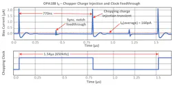
Choosing lower-impedance feedback and source impedances and including output filtering can virtually eliminate both offset shift and noise tone issues. The application note, “Optimizing Chopper Amplifier Accuracy,” explains the topic in detail and provides design recommendations.
What Factors are Reducing the Cost of Precision Analog?
Zero-drift and e-trim technologies are two design approaches that help reduce component and system costs. Both use CMOS devices because they require digital control or communications. For zero-drift devices, the savings occur since no trimming is needed, as the device employs a fixed internal calibration scheme to minimize offset. Laser trimming can be fairly expensive because it’s a time-consuming iterative semiconductor test process.
The test time for semiconductor devices accounts for a significant portion of device costs — semiconductor testers are expensive, and that expense needs to be amortized across the life of the tester. Zero-drift devices require no trimming. The trimming time for e-trim devices will increase test times somewhat compared to zero-drift devices. However, the test-time increase for e-trim devices is minimal because the process uses a digital command to the device, whereas laser trimming is an iterative series of laser cuts in the resistor, which takes more time than e-trim.
As a general trend, the wafer size in modern wafer fabrication plants has increased, while there’s been a decrease in die size. This yields more die manufactured per wafer, which also helps lower costs. In some cases, reducing die size with some performance compromise can further optimize costs.
For example, the output transistors on most amplifiers take up a large portion of the die area. Reducing these transistors can significantly reduce costs, but there will be some compromise on output current and output swing to the rail. In general, eliminating features by making tradeoffs on specifications can help shrink die size and cost.
How Can Precision Analog Save Money?
Even with the substantially reduced cost of some modern precision devices, many designers will still choose the lowest-cost general-purpose devices. This can be a reasonable approach to lowering cost, but the general-purpose device will have significant accuracy tradeoffs.
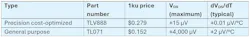
For example, the TLV888 from TI is a precision cost-optimized zero-drift device, while TI’s TL071 is a general-purpose device first released in 1978. The cost of both devices is quite low, but the general-purpose device is roughly half the cost of the cost-optimized precision device.
Figure 5 summarizes the primary specifications for these two devices. The precision device is hundreds of times better than the general-purpose device for VOS, VOS drift, and other parameters. In some cases, the specifications may not be a priority — cost is the main target. Keep in mind, however, that there may be some hidden expenses in using less-precise devices.
One hidden expense is calibration. Factory calibration is done by precision test signals to the input of your amplifier signal chain, and by measuring the gain and offset of that signal chain. The gain and offset errors are unique for each device and will generate a unique set of calibration coefficients. Typically, the calibration coefficients are stored in the system’s EEPROM and are used to compensate for post-calibration errors. This method works well, but it can significantly increase the test time and complexity of the end product.
Furthermore, calibration normally occurs only at room temperature, so the temperature drift of the device isn’t corrected. Using precision devices in a signal chain is a common approach to eliminate the need for calibration.
Another hidden expense can be design and debugging time. A precision device is much closer to the ideal op amp than most general-purpose devices, which may have many different nonidealities that must be considered. Taking care to avoid the specification limitations takes skill, understanding, and analysis time. Designing with precision devices will generally be easier than with devices that carry significant limitations.
Finally, because precision devices have better specifications, they’re more universal. For example, you may be able to use one or two different precision amplifiers to meet the requirements for a particular product, but it needs many different general-purpose devices for the same product. Again, this is because the precision device is closer to the ideal op amp and is usable for more applications. Reducing component count will simplify your bill of materials and inventory control.
Why is There a Need for a Premium Device?
While there is still a premium class of devices, modern technology advances are enabling precision devices at a lower cost. The additional costs can often stem from the increased die size needed to achieve the device’s primary specifications.
For instance, an op amp that can deliver a lot of current will need large output transistors. Low-noise op amps require large input transistors. Bipolar devices often have to be laser trimmed, which will add test time and cost. Premium devices may use a special process to achieve higher power-supply voltages and other special characteristics. For modern analog designs, there are options for very low-cost general-purpose devices, precision cost-optimized devices, and premium precision devices.
Though there aren’t many details at press time, TI is quietly releasing a new precision op‑amp portfolio today, July 1, 2026, in China, which blends performance, innovation, value, and scalability for low- and high-voltage needs.
Here’s a literal excerpt of the op-amp portion from a multi-product press release we received on my request:
- Designed for industrial, data center, and precision‑measurement markets, TI’s latest family of operational amplifiers is enabling cost-optimized high-accuracy performance. The new portfolio provides low offset (sub‑100 µV), low drift, and low noise operation across supply voltages from 1.7V to 36V.
- Featuring a range of devices with zero-drift technology, which actively cancels offset and drift to as low as 5 nV/°C, and the patented e-TrimTM post-packaging trimming to provide stable offset and low input bias currents without field calibration, this portfolio helps engineers improve overall system reliability and accuracy.
- Spanning many gain bandwidth, rail-to-rail, output-drive, and slew rate configurations across a wide supply-voltage range, the new portfolio delivers scalable design across a variety of market segments.
- The family offers a range of reliable, high‑precision solutions that factor in cost and design considerations, joining TI’s extensive offerings of general-purpose and high-precision operational amplifiers. Visit TI's website for more details.
Thanks to Art Kay for likely spending his weekend writing up his related article for us upon short notice.
—andyT
>>Download the PDF of this article, and check out the TechXchange for similarly themed articles and videos
About the Author

Art Kay
Application Engineer, Texas Instruments
Art Kay is an application engineer in the precision amplifiers team at Texas Instruments. He specializes in the support of low-noise data-acquisition systems, and has published a book on intrinsic noise analysis. He also co-published a useful summary of analog engineering relationships (TI’s Analog Engineer’s Pocket Reference) and a companion software tool. Art was instrumental in the development of an online training program for amplifiers and data converters, and has conducted many live seminars on the subject.
Before working in applications engineering, he was a semiconductor test engineer for Burr-Brown and Northrop Grumman Corp. Art graduated from Georgia Institute of Technology with a MSEE and from Cleveland State University with a BSEE.
Comment About the Article
To join the conversation, and become an exclusive member of Electronic Design, create an account today!

Leaders relevant to this article: