An Amateur’s View on the P2 (Part 3): Diode Bridge and Gain Adjust
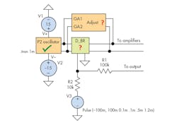
1. This simplified block representation shows the interaction between the oscillator, diode bridge, P2 inputs, and gain/phase adjust interact.
After a concise investigation on the P2’s oscillator and slew-rate response in Part 2, we proceed with the diode bridge and offset adjust blocks (Fig. 1). A diode bridge can be configured as a double balanced modulator/mixer by adding transformers that “multiply” the signals, forming two sidebands. Remember that we can represent the trigonometric functions sin(x) or cos(x) with their complex exponential counterparts (Fig. 2).
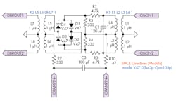
2. Here’s the internal schematic of the P2 diode bridge.
When we do this for the product of two trigonometric functions and simplify, we end up with the sum of two trigonometric functions whose frequencies have been added and subtracted to each other. Therefore, we expect the output of the diode bridge to be a resultant wave composed of f1+f2 and f1−f2, given that f1 and f2 are the frequencies of the two input signals to the bridge. By doing this, dc-related noise is significantly reduced (since information from the input signal is now “encoded” in ac).
To get a better feel of the diode bridge, I prepared the test setup shown in Figure 3.
3. Diode bridge test schematic for Case 1.
The inductors provide dc isolation, with a coupling coefficient of 1. Diodes D1, D2, D3, and D4 are identical, modeled with a zero-bias junction capacitance of 105 pF [default=0] and saturation current of 3 pF [default=0.01 pA]. The signal entering OPAMPIN+ to OPAMPIN− will be superimposed on the signal entering OSCIN1 to OSCIN2. The output is at DBROUT1, with its 180° phase-shifted version at DBROUT2.
Coupling 5-MHz and 1-kHz Sinusoids with the Diode Bridge
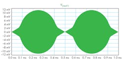
First, I test what will happen when I feed a 1-kHz and a 5-MHz sinusoid to the diode-bridge block of the P2. Signal source/generator SS1 will supply the 1-V p-p, 1-kHz sine wave while SS2 will provide a 5-MHz signal of equal amplitude. I am theoretically expecting a signal with pronounced frequency components at 5 MHz + 1 kHz and 5 MHz − 1 kHz. Simulating yields the VOUT1 waveform in Figure 4.
4. This is the simulation result of VOUT1 for the test schematic in Fig. 3.
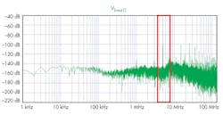
Using the fast Fourier transform (FFT) to observe the frequency spectrum of VOUT1 yields the results shown in Figure 5.
5. A fast Fourier transform was used to observe the frequency spectrum of VOUT1.
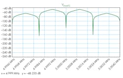
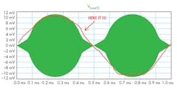
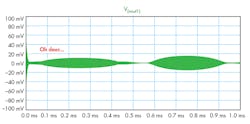
From the FFT plot, it’s clear that the peaks are at 4.999 MHz and 5.001 MHz, verifying our theoretical expectations (Fig. 6). Furthermore, the information in VSIG1 is visible at the envelope of VOUT1 (Fig. 7). Can you see it?
6. A zoomed-in view on the peaks of the FFT curve in Fig. 5.
7. Where is the information of VSIG1?
Now we have an ac signal with information “riding” on it. All we have to do is amplify and then demodulate it before the output. Right? Not yet. There’s one more bit of housekeeping that needs meticulous attention—the diodes we choose for the bridge.
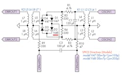
What happens when the diodes are mismatched? Below, I’ve declared a new diode model, V48, with its saturation current at 7 pA and zero-bias junction capacitance at 205 pF (Fig. 8).
8. Here, the P2 diode bridge schematic was modified. D2 has been mismatched.
Mama Mia! What has happened to our output (Fig. 9)? Can you imagine, increasing the saturation current by just 4 pA and the capacitance by 100 pF having such an effect on the output? To ensure that choice of values wasn’t a factor, I matched all of the diodes again using V48, re-simulated, and got the proper waveform. It certainly must have been a daunting task to manufacture the P2 with four diodes that had such stringent matching conditions.
9. Shown is the simulation result of Fig. 8.
This isn’t the only instance where matching played a crucial role in design. I believe the same rule applies for Kelvin bridges, or any similar circuit configurations, with the only difference being a more relaxed demand in accuracy. How about current mirrors, which must have MOS pairs that are identical to each other, or else the “mirrored” currents would have offsets?
This block isn’t the only one controlling the gain of the oscillator. Remember the C40 capacitor encircled in red back in Part 1? I think it’s meant to provide feedback from the ac demodulator (which makes sense—how can you demodulate/decode something if you have no idea or information on the code or original content used?) This discussion, however, is for a future article.
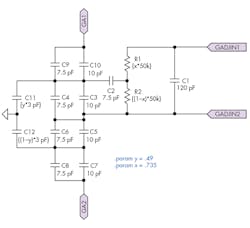
10. This schematic illustrates offset adjustment in the P2.
Observing the resistor-capacitor network in Figure 10, C11 and C12 are most probably variable capacitors, while R1 and R2 are potentiometers. Terminals GA1 and GA2 connect back to the oscillator while GADJIN1 and GADJIN2 connect to the outputs of the diode bridge. From Part 2, we recall the most interesting component of the oscillator, C6, where the value of capacitance and amplitude of oscillation share an inversely proportional relationship, valid from 25pF to 1µF, after which oscillation stops.
Looking back at Fig. 10, I believe it’s safe to assume that the capacitance will only vary in the picofarad range because series-parallel connections will cancel each other out. We should be surprised if we saw a capacitor here with a value of 1µF or more.
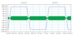
To conclude, let us simulate the schematic in Fig. 1 (Fig. 11).
11. A simulation of the Fig. 1 setup produced this result.
Node 2 is the output of the diode bridge (shunted to the offset adjustment block). Node 7 is the input pulse to the diode bridge. Different combinations of x and y yield different results (less than 1, of course). When x and y are at very low values, the peak-to-peak voltage of node 2 approaches that of node 7. I think the default values set in Fig. 10 are just right to prevent overmodulation.
Can you see the information riding on node 2?
About the Author
Justin Mamaradlo
Engineer
Justin Spencer D.L. Mamaradlo is an electronics engineering graduate of the University of Santo Tomas, the Royal and Pontifical university of the Philippines and the oldest university in the country. During his academic years, he specialized in communications and networking technologies and was recognized in the Dean's list. He passed the government license examination with the second highest average in his batch. He is currently working in the semiconductor industry
Aside from a thirst for knowledge and innovation in electronics, he also likes playing classical piano and guitar. He occasionally volunteers for environmental causes with Greenpeace and is an enthusiastic learner of formal chess.
