Build a Flyback-Based Geiger Counter with LabVIEW Interface

This article discusses radiation particles and gives a summary of their effects. We will create a Geiger counter circuit based on the flyback circuit that was the focus of the article “Take A Flier on the Flyback for Your High-Voltage Circuit Design,” and will interpret the data with a LabVIEW graphical user interface. Also discussed is how the Silego GreenPAK, a configurable mixed-signal IC (CMIC), can be used to implement all analog and digital functionality to drive a high-voltage Geiger tube, count the discharge events, and communicate with a personal computer via LabVIEW.
How a Geiger Tube Works
The Geiger-Muller (GM) tube allows a user to measure different types of radiation, including alpha, beta, x, and gamma particles. A GM tube consists of one anode and one cathode enclosed in a cylindrical box. The cylinder contains some low-pressure gas, usually about 0.07 to 0.13 bar. One side of the tube is non-metallic, and is generally made of a thin mica foil window.
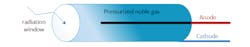
1. Geiger-Muller tube structure contains two electrodes.
As seen in Figure 1, two electrodes are present. When a high voltage is applied to the anode and cathode, a strong electric field is generated inside the GM tube, which contains a low-pressure noble gas (typically argon). When no radiation is present, the noble gas acts as a non-conducting medium. However, when a particle crosses the GM tube, the pressurized gas becomes ionized, and that starts an avalanche effect. This means that the noble gas begins to conduct, and a current can flow through the GM tube toward the detector circuit.
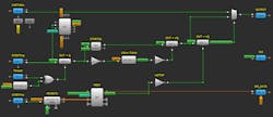
Schematic Block Architecture
Figure 2 shows the main blocks of the proposed Geiger counter circuit. The circuit control unit is the Silego GreenPAK CMIC IC, which implements all of the logic functions and analog processing of the external signals. A 5-V power supply must be used for the circuit to operate properly. For this demonstration, the GreenPAK IC is powered separately by the Silego development board, which is connected to a PC with an USB cable.
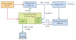
2. Shown is the general architecture view of the Geiger counter circuit.
We used the same flyback unit that was discussed in the aforementioned “Take a Flier on the Flyback for Your High-Voltage Circuit Design” article. It’s composed of a transformer, a rectifier diode, and a few other passive components. The high voltage on the Geiger tube is then scaled by a resistor divider and fed to the GreenPAK’s analog comparator. Here, the analog signal is processed and used to generate the PWM signal for the flyback unit. The duty cycle of the PWM signal is regulated to achieve the desired high voltage on the flyback output.
When a radiation particle strikes the Geiger tube, an internal discharge takes place. This leads to a temporary voltage drop on the flyback unit output. This voltage drop triggers a circuit detector that generates a low-voltage pulse for each discharge and, thus, for each particle against the Geiger tube walls. The low voltage pulse is fed to a digital counter inside the GreenPAK that counts the number of events. Finally, the value of the digital counter is sent to the LabVIEW GUI through the GreenPAK’s serial peripheral interface (SPI) block. A UART-to-USB bridge is used to send the counter information from the GreenPAK to the PC running LabVIEW. An external button is used to reset and initialize the event counter.
Simulation
Before constructing the circuit, we simulated the entire design in order to provide the exact waveform to the components. Since parts of the design deal with high-voltage values, the design must work as intended to avoid system or component issues.
In the article on the flyback circuit, we configured the circuit to reach a value of at least 450 V. Now, we will simulate the interface with the Geiger tube.
In Figure 3, the linking point is labeled “HV” in the center of the schematic. The flyback circuit is highlighted by the red square. We implemented the interface with the GreenPAK for pulse detection.
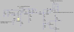
3. The red square indicates the flyback in this simulation circuit.
To simulate the Geiger Tube and the pulse generated by a particle striking the tube, we decided to use a simple switch (S1) with a RDS(ON) of 1 kΩ, which is activated by the V3 pulse generator. It creates a pulse that’s delayed by 35 ms, and waits for the correct circuit polarization of the flyback portion. Once the voltage value reaches the correct amount, a 1-µs pulse is generated and the switch closes. A path from HV to GND is formed and the pulse can pass the C5-R7-R10 high-pass filter, reaching the base of the transistor Q1.
The two transistors are configured as a Darlington pair, and they provide a current proportional to their hFE and the current at the base of Q1. This way the collector of Q1 and Q2 will start at the supply voltage of 5 V and decrease down to 0, providing a pulse to the GreenPAK.
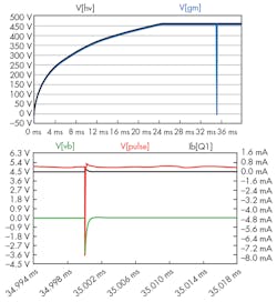
4. On top is the high-voltage path and Geiger tube discharge. Below that is a plot for the current at the base of transistor Q1 and the output voltage pulse.
As seen in Figure 4, the flyback reaches 450 V and is ready to polarize the Geiger tube. Once the event occurs, the voltage at the Geiger tube goes low. The current at the base of the transistor increases, the output current follows the base current, and the output voltage rapidly goes down.
GreenPAK Implementation
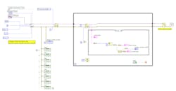
In this section, we will explain how the event counter and UART transmission are implemented inside the Silego GreenPAK. Figure 5 shows the overall architecture of the logic implementation. The pulse generated from the Geiger circuit is connected to pin 7. The signal, labeled EVENTtrig, drives the event counter (CNT2) and the D flip-flop (DFF1). The EVENTtrig is passed to CNT2 through the EXT CLK 0 line of the oscillator block (OSC).
5. Shown is the overall logic architecture of the GreenPAK implementation.
When an event occurs, the rising edge increments the event counter and sets the Q output of the DFF1 labeled txSTART. When txSTART goes high, the CNT5 reset signal goes low through inverter 2-L1. This means that the CNT5 output starts to generate a clock pulse with a period of 104 µs used to synchronize the UART transmission with a baud rate of 9600.
Before the CNT5 triggering, the counter output is HIGH. This means that the reset signal (DFF0 nRES) is LOW and thus the DFF0 output is held HIGH. For this reason, a delay is needed (Pipe Delay0) between the DFF1 output and the DFF0 clock input. Figure 6 highlights why the delay is necessary.
If we drive the DFF0 clock input directly with the txSTART signal, the DFF0 nRESET pin will be low and the DFF will be disabled when a rising edge occurs on its CLK pin. The delayed start (pink trace, Fig. 6) appears when the nRESET signal goes HIGH, which enables DFF0. Once that occurs, the STARTdly signal will set the output of DFF0 (nQ) LOW.
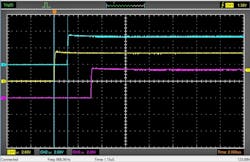
6. Start trigger and start delayed signals. The yellow waveform trace (channel 1) is txSTART, the blue trace (Channel 2) is the DFF0 reset signal (UARTclk/CNT5 output), and the pink trace (channel 3) is STARTdly.
After 104 µs, CNT5 generates a pulse on its output. The rising edge of this pulse will reset DFF0, bringing the nQ HIGH again. Consequently, DFF0’s output will set DFF2. This means that the SPI chip-select signal goes LOW and the SPI starts to transmit the CNT2 stored value with a clock period of 104 µs. The DATA/START/STOP signal will select the UARTdata signal on the output multiplexer. When the last bit is sent, the INT signal of the SPI module will reset the DFF2 through the inverter 2-L0 (txSTOP signal). The DATA/START/STOP signal goes back HIGH again and selects the HIGH logic level on the START/STOP line (STOP condition).
At the same time, the SPI interrupt signal (labelled TXrestart) resets CNT6/DLY6, which is passed through 2-L2 to enable DFF1. This allows a new transmission to take place. PIN5 resets the event counter while PIN6 is a manual UART transmit restart.
Figure 7 shows the clock signal (light blue), the event trigger signal (yellow), and the UART data (pink). The SPI transmits the most-significant bit (MSB) first. A bit order inversion will be performed on the LabVIEW interface to achieve a least-significant bit (LSB) first value.
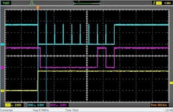
7. These UART transmission signals include the clock signal (light blue), the event trigger signal (yellow), and the UART data (pink).
It’s very important to highlight that during transmission, the event counter is free to count new incoming events and doesn’t block the value related to the start of transmission. As you can see, the event counter is directly connected to the event pulse signal (PIN7).
UART-to-LabVIEW Communication
To communicate between the GreenPAK and a laptop, we used a Silicon Labs CP210x UART-to-USB bridge. Pin TX of the USB bridge is connected to pin 8 of the GreenPAK. Pins 9 and 10 of the GreenPAK are shorted together, and the ground is shared (Fig. 8).
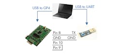
8. A UART-to-USB bridge is key to this board configuration.
Once everything is set up, we can start up LabVIEW and open the user interface (Fig. 9). After linking the devices to the USB port, you have to select the correct COM port. In our case, the corresponding COM port was COM3. Once the START button is pressed, the program will wait for incoming communication. The LED represents the single bit counting output, and the Geiger counter events display shows the total number of events from the start of the communication. The STOP button blocks the communication and closes the program.
9. After setup, the LabVIEW program can be initiated.
When you open the front panel, you can see the user interface with the LabVIEW controls (Fig. 10). UART communication is initialized with a baud rate of 9600. The packet size is 8 bits long, plus one start and one stop bit. No termination characters, parity bits, or flow-control bits are necessary. All bits are set to default values to avoid erroneous visualization due to the previous acquisition.
The Geiger counter events display is set to zero. The VISA buffer is set to one byte, which the device receives during communication. Once the link is established, the program enters the while loop and waits for an incoming transmission from the GreenPAK. The string buffer is converted to single bits and reversed, since the GreenPAK SPI sends the data MSB-first and we need to read the data LSB-first. After that, the received data is converted to an integer value and displayed. When the STOP button is pressed, the program exits from the while loop and the communication is closed.
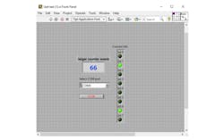
10. LabVIEW controls enable you to see the user interface.
In this video, you can see the counter on the display incrementing when a button is pressed in the emulator interface, which simulates a trigger event.
Conclusion
This article shows how to use the Silego GreenPAK’s analog and digital blocks to implement standard UART communication. The design simulates and analyzes complex events and delivers a precise flyback SMPS with few components. This combination of elements enabled us to create a Geiger counter with a LabVIEW interface, which measures radiation in real time.

About the Author
Michele Marino
Analog & Mixed-Signal Designer
Michele Marino received a Master’s in electronic engineering at “La Sapienza” University in Roma. Presently he’s working as Analog & Mixed Signal designer at LoMi Electronics.
Lorenzo Massari
Mixed-Signal and LabView Developer
Lorenzo Massari received a Master’s in digital electronics engineering. Presently he’s working as Mixed-Signal and LabView developer at LoMi Electronics.
Comment About the Article
To join the conversation, and become an exclusive member of Electronic Design, create an account today!

Leaders relevant to this article: