How to Control EMI in Synchronous Buck Converters
This file type includes high-resolution graphics and schematics when applicable.
When converting a higher voltage to a lower voltage, a buck (switching) converter provides much greater efficiency than its linear counterpart. Buck converters can achieve efficiencies of 95% or higher, far surpassing linear regulators, which typically fall in the 40% range.
The basic buck converter (Fig. 1a) consists of a MOSFET switch (S1), diode, output inductor (L), and output capacitor (C). During operation, S1 alternates between the closed (on) and open (off) states. When S1 is closed, the input voltage is connected to the load through the inductor, which stores energy in its magnetic field. The capacitor is charging, and the output voltage begins to rise toward the input voltage. The diode is reverse-biased.
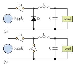
When S1 is opened, the magnetic field collapses, causing a negative kickback voltage across the inductor. This turns on the diode, which performs a flyback function, allowing current to flow around the L-C-D loop as the inductor returns its energy to the circuit. The inductor initially also provides energy to the load. When this is exhausted, the capacitor supplies the load and the output voltage begins to decay. Then the switch is closed again and the sequence repeats.
The value of the output voltage is given by: VOUT = VIN * tON/(tON + tOFF). A 50% duty cycle (tON = tOFF ) will, therefore, give an output voltage half that of the input. The output also exhibits a ripple caused by the charging and discharging of the capacitor.
The synchronous buck topology (Fig. 1b) is a refinement of the basic design. It replaces the diode with another transistor switch (S2), which is turned on when the diode in Fig. 1a would normally be conducting. The power dissipation of a MOSFET is less than a diode, so this change increases efficiency. The control circuit must make sure that both S1 and S2 aren't on simultaneously, a condition known as “shoot-through” that effectively shorts the power supply to ground. To avoid this, a “dead time” is added between one FET turning off and the other FET turning on.
Switching Converters and EMI
Synchronous buck converters are widely used in industrial, consumer, and automotive applications, but as power-supply efficiency becomes more important, designers have turned to faster switching speeds—as high as 10 MHz—to reduce losses. A faster switching speed, though, brings with it an increase in electromagnetic interference (EMI), which can have undesirable results. In an automobile, for example, excessive EMI could generate audible noise in the car stereo, or even cause a malfunction in a safety-related system.
What are the causes of switching-converter EMI? The fast edges of the voltage waveforms contain high-frequency harmonics, which are easily coupled into other circuits (conducted EMI).
The high-frequency energy can cause significant voltage overshoots and induce ringing in the resonant parasitic circuits in the design. The ringing magnitude is a function of the switching speed of the high-side MOSFET and the stray inductance in the layout and packaging. In extreme cases, the voltage magnitude of this ringing can exceed the absolute maximum drain-to source voltage of the low-side MOSFET.
Circuit Modifications to Reduce Ringing and EMI
The circuit in Figure 2 shows the power-stage components for a synchronous buck converter. It includes the basic components in Fig. 1b—the MOSFET power switches S1 and S2, output inductor, output capacitor and load. It also shows the parasitic inductances and capacitances that cause switch-node ringing, as well as some additional components that can lower the magnitude.
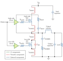
Figure 2 depicts three circuit modifications that can reduce switch-node ringing: a boot resistor, high-side gate resistor, or snubber. They aren't mutually exclusive, so more than one can be used in the same design. For best results, these modifications should always be used in conjunction with good layout practices.
Option 1: Add a Gate Resistor
Perhaps the simplest option is to reduce the high-frequency energy available for causing mischief by adding a resistor RGATE in series with the gate of the high-side (HS) MOSFET. This relies on the fact that the isolated gate electrode of a MOSFET forms a capacitor (CGS) that must be charged or discharged each time the MOSFET is switched on or off. A series gate resistor combines with CGS to form a RC low-pass filter, slowing down the turn-on and turn-off of the MOSFET.
This has the advantage of simplicity, but reduces efficiency by increasing switching power loss. In addition, the main EMI benefit accrues from increases in the turn-on time of the HS MOSFET; i.e., slowing down the rising edge. Adding the gate resistor slows down both transitions. A reverse diode can be placed in parallel with the resistor to speed up the turn-off (Fig. 3).
Although it's not as important for EMI reductions, a gate resistor in the low-side (LS) MOSFET circuit can still play a useful role.
In Figure 2, RGATE2 acts to increase the time that it takes for the LS MOSFET to turn off. Slowing down the turn-off time increases overall efficiency by decreasing the dead time. After the HS MOSFET turns off, the LS MOSFET conducts inductor current through its internal body diode until it turns on. The internal body diode typically has a high forward-voltage drop, which can lead to a significant reduction in overall efficiency.
One caution: When reducing the dead time for a synchronous buck, remember that there's part-to-part variation, so leave an adequate margin to avoid the risk of shoot-through.
Option 2: Add a Snubber
A second option is to add a snubber (RSNUBBER and CSNUBBER in series) from the switch node to ground. The snubber circuit dampens parasitic inductances and capacitances during switching transitions, thus reducing the ringing voltage and frequency as well as reducing the number of ringing cycles. This helps lower the EMI emitted by the system.
A fully optimized snubber can be designed to allow a defined amount of overshoot and then settle with minimum energy loss given the overshoot requirement. One drawback is that board-to-board variation is large enough to frustrate this noble goal. Calculating the values of the snubber components is an iterative process that includes empirical testing.
The procedure starts with an estimate of the parasitic circuit inductance and switch-node capacitance. Once these are determined, the snubber resistor value is calculated to give a damping ratio of close to unity for fast rise time and minimal overshoot. Next, the snubber capacitance is chosen to provide a balance between control of the ringing and desired power loss. Finally, the selected values are empirically tested and modified as necessary.
More detail on snubber calculations is available in this application note.
Option 3: Use a Boot Resistor
The charge-pump circuit in Figure 2 uses CBOOT to boost the HS gate supply above the supply voltage of the power stage. A boot resistor (RBOOT) in series with the capacitor can reduce ringing by slowing down the turn-on of the HS FET. The slower turn-on allows more time for the parasitic network to discharge, limiting the ringing. The value of the boot resistor is determined empirically; start at 0 Ω, then increase the resistance until the ringing is reduced to the desired level.
The boot resistor affects only the turn-on of the HS MOSFET, making this method an efficient way to reduce ringing. However, if the boot resistor is too large, the boot capacitor may not get fully charged in each cycle. Then the gate driver would not have sufficient voltage to keep the HS MOSFET on and could turn off in mid-cycle. This restriction limits the size of the boot resistor and, hence, the reduction in ringing achievable with this method.
Option 4: Use an Integrated Solution
Several manufacturers offer synchronous buck converters with integrated features to help with EMI reduction. TI's LM5140-Q1, for example, is an automotive-qualified part that features adjustable slew-rate control to simplify compliance with automotive EMI requirements such as CISPR 25. The standard covers radiated and conducted emissions in the 150-kHz to 2.5-GHz frequency range.
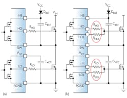
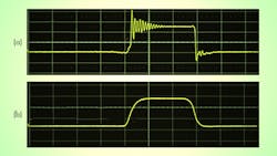
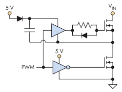
Figure 4 shows the output stage of the LM5140 compared to that of a standard converter. The standard converter (Fig. 4a) has the HS and LS driver pairs connected internally, allowing for only a single gate resistor for each power FET. In the LM5140 (Fig. 4b), each driver FET is pinned out separately, allowing for individual turn-on and turn-off control of each HS and LS power transistor.
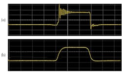
Providing individual slew-rate control of each switching transition allows the designer to optimize performance for each application. The basic buck converter from Figure 4a exceeded the limits for the CISPR 25 Class conducted emissions test by 15 dBµV in the 30- to108-MHz frequency range. As shown in Figure 5, adding slew-rate control eliminated switch-node ringing and allowed the design to pass the test.
Conclusion
Synchronous buck converters enable high-efficiency power conversion, but conducted and radiated emissions are ever-present concerns, especially with increasing switching speeds. We've discussed several useful techniques for dealing with this problem. When combined with best-practice board-layout techniques, they can reduce emissions to levels that allow switching converters to be used in EMI-sensitive automotive, industrial, and consumer applications.
Looking for parts? Go to SourceESB.
About the Author
Paul Pickering
Paul Pickering has over 35 years of engineering and marketing experience, including stints in automotive electronics, precision analog, power semiconductors, flight simulation and robotics. Originally from the North-East of England, he has lived and worked in Europe, the US, and Japan. He has a B.Sc. (Hons) in Physics & Electronics from Royal Holloway College, University of London, and has done graduate work at Tulsa University. In his spare time, he plays and teaches the guitar in the Phoenix, Ariz. area
Comment About the Article
To join the conversation, and become an exclusive member of Electronic Design, create an account today!

Leaders relevant to this article: