Lens-on-MEMS Assembly Enables Flat Optics, Dynamic Steering

As electronic devices get smaller, lighter, and thinner, the associated optics must do the same. Fortunately, some of the technologies of electronics are also applicable to optics, and vice versa, as demonstrated by a recent collaborative effort between Argonne National Laboratory and Harvard University. The team integrated two technologies—microelectromechanical systems (MEMS) and metalenses—to design and produce a lens that sits on top of a steerable platform and can be made with the same technology used to fabricate ICs.
The project is described in an article in APL Photonics, “Dynamic metasurface lens based on MEMS technology.” Additional fabrication and characterization details are in a Supplementary Information document. The complete device measures just 900 microns in diameter and 10 microns in thickness; a two-dimensional (2D) scanning MEMS platform controls the angle of the lens along two orthogonal axes by up to about ±9° each, which enables dynamic beamsteering. Potential applications include miniaturized microscope systems, LiDAR scanners, and projection systems.
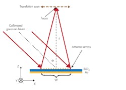
1. The metasurface lens functions as a focusing reflective surface when illuminated by a collimated beam. (Source: Argonne National Laboratory/Harvard University)
By using the metasurface itself to separate the incident and reflected beam paths, there’s no need for a beam splitter, thus eliminating one of the bulky optical components often used in optical systems. Figure 1 shows a schematic of the reflective metasurface lens when a collimated, incident Gaussian beam at angle θ is focused at a distance f along the normal axis to the lens surface.
The metasurface lens mirrors, also called resonators or cells, are fabricated using standard photolithography techniques on a silicon-on-insulator (SOI) wafer with a 2-μm-thick top-device layer, a 200-nm buried-oxide layer, and a 600-μm-thick handle layer (Fig. 2).
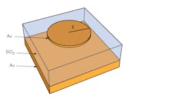
2. Each unit cell of the metasurface lens consists of a 50-nm-thick gold disc on 400-nm-thick silicon-dioxide substrate with a 200-nm-thick gold backplane. (Source: Argonne National Laboratory/Harvard University)
The mirror dimensions are 1 × 1 mm and a thickness of 10 μm; resonance is about 1 kHz for each torsional axis. The actual details of the metalens/MEMS fabrication and attaching the cells to the MEMS surface are impressive; the paper and supplement provide the details. The MEMS cells have varying diameters from 1.2 to 2.0 μm, so they can be tightly packed onto the planar surface (Fig. 3). They reflect mid-IR light (λ = 4.6 μm), which the metalens focuses without need for additional optical components, such as a focusing lens.
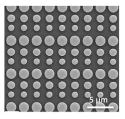
3. This scanning electron microscope (SEM) image of the fabricated lens shows the varying sizes of the mirror cells, used to create the desired lens-plane density. (Source: Argonne National Laboratory/Harvard University)
The 2D scanner with integrated flat lens is actuated by electrostatic vertical “comb” drives, which are interdigitated stationary and rotating plates. Applying a voltage between these plates causes the moving elements to be pulled downward, causing rotation around an axis (Fig. 4).
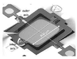
4. This SEM shows a bare MEMS platform with a square layout with each side measuring 900 µm; the gimbal axes are called out. (Source: Argonne National Laboratory/Harvard University)
The micromirror is electrostatically rotated about its inner axis using the vertical comb drives mounted on the gimbal frame, while the gimbal frame itself rotates about the outer axis using the vertical comb drives mounted on its frame and substrate. This is analogous to the gimbaling used on a two-degree-of-freedom mechanical gyroscope. The finished device is mounted in a DIP package.
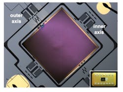
5. This optical-microscope image of a MEMS scanner with a flat lens on top also indicates the two rotational axes of the scanner; the inset shows the device mounted on a dual-in-line (DIP) package ready for wiring and electrostatic actuation. (Source: Argonne National Laboratory/Harvard University)
The prototype lens assembly, consisting of 374 cells of varying diameters (Fig. 5), was designed to be “perfectly” flat. But, of course, that’s not the case; its curvature was measured using an optical profilometer. The reflected beam path is at 0.5° compared to the designed value of 0°, and the full width at half maximum (FWHM)—analogous to the 3-dB bandwidth in electronics—becomes wider, at 41.7 µm compared to 22.8 μm.
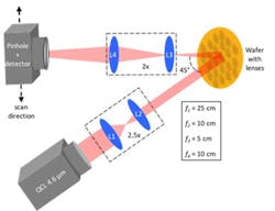
6. This experimental arrangement was used for characterization of the optical response of the “flat lens.” (Source: Argonne National Laboratory/Harvard University)
The optical focusing performance was also evaluated using incident light (laser at 4.6 μm) with a beam only slightly larger than the 800-μm square lens and angled at 45° to the unactuated scanner. The profile of the reflected focal line was measured for three positions of the MEMS platform (Fig. 6).
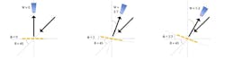
7. In the three experimental test configurations, the MEMS scanner is actuated to move the lens by rotational angles of 0°, 1°, and 2.5°, respectively, while the angle of the incident illumination remains unchanged. To align with the peak of the reflected signal, the position of the detector needs to be at 0°, 2.7°, and 7.3°, respectively. (Source: Argonne National Laboratory/Harvard University)
Voltages of 0 V (unactuated), 40 V, and 60 V were applied across the outer axis so that the lens tilts by 0°, 1°, and 2.5°, respectively (Fig. 7). The corresponding measured FWHM of the focal lines for the three tilted positions of the lens are shown in Figure 8.

8. Shown is the measured FWHM of the focal lines for the three tilted positions of the lens in Fig. 7. (Source: Argonne National Laboratory/Harvard University)

About the Author

Bill Schweber
Contributing Editor
Bill Schweber is an electronics engineer who has written three textbooks on electronic communications systems, as well as hundreds of technical articles, opinion columns, and product features. In past roles, he worked as a technical website manager for multiple topic-specific sites for EE Times, as well as both the Executive Editor and Analog Editor at EDN.
At Analog Devices Inc., Bill was in marketing communications (public relations). As a result, he has been on both sides of the technical PR function, presenting company products, stories, and messages to the media and also as the recipient of these.
Prior to the MarCom role at Analog, Bill was associate editor of their respected technical journal and worked in their product marketing and applications engineering groups. Before those roles, he was at Instron Corp., doing hands-on analog- and power-circuit design and systems integration for materials-testing machine controls.
Bill has an MSEE (Univ. of Mass) and BSEE (Columbia Univ.), is a Registered Professional Engineer, and holds an Advanced Class amateur radio license. He has also planned, written, and presented online courses on a variety of engineering topics, including MOSFET basics, ADC selection, and driving LEDs.
Comment About the Article
To join the conversation, and become an exclusive member of Electronic Design, create an account today!

Leaders relevant to this article: