Low-Power 12-bit ADC for 5G, Radar Boosts Sampling Rate

The relentless push of analog-to-digital converters (ADCs) that can meet the extreme demands of leading-edge applications, including 5G instrumentation and oscilloscopes, or provide direct sampling for X-band radar design, continues with the introduction of Texas Instruments’ dual-channel ADC12DJ5200RF IC (Fig. 1). Texas Instruments will have an array of its latest products, including ADCs, at the 2019 IMS exhibition, at Booth 1272. The IC delivers what the company maintains are the widest bandwidth, fastest sampling rate, and lowest power consumption specifications available today.
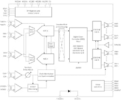
1. The Texas Instruments ADC12DJ5200RF dual-channel, 12-bit, 5.2-Gsample/s/channel ADC targets 5G and related applications.
Among its specifications, this converter boasts:
• An 8-GHz analog-input bandwidth, 20% better than competing ADCs, which may eliminate the need for an additional down-conversion stage in some designs.
• 5.2 Gsample/s sampling per channel with instantaneous bandwidth of 2.6 GHz (at 12 bits). When used in single-channel mode, these numbers double to a sampling rate of 10.4 Gsamples/s and instantaneous bandwidth of 5.2 GHz. ENOB (effective number of bits) in dual-channel mode (at FIN = 2.4 GHz) is 8.6 bits.
• A ”slim“ and fast serial interface using the JESD204C standard under various encoding modes, with 16 serialized lanes supporting up to a 17.16-Gb/s line rate for efficient data transfer to the associated processor/FPGA.
These basic specifications are only part of the story. The ADC12DJ5200RF, with its full-scale input voltage of 0.8 V p-p, features a low noise floor of –151.8 dBFS/Hz (dual-channel mode) and –154.4 dBFS/Hz (single-channel mode). It also adds innovative synchronization features, including a “noiseless” aperture-delay adjustment and timing-reference windowing to simplify system design of higher channel-count applications. The high-resolution 19-fs/step sampling control eases synchronization and interleaving across multiple channels while accommodating temperature- and voltage-invariant delays.
Power dissipation and footprint are always important issues for these gigahertz-class ADCs. The device’s 144-ball, 10- × 10-mm flip-chip BGA is 30% smaller than discrete solutions, while the reduced number of JESD204C lanes enables a smaller overall PCB design. The 4-W power consumption from 1.1- and 1.9-V rails is 20% lower than competitive ADCs, according to TI. To provide a smoothed upgrade path from existing lower-speed TI ADCs (beginning at 2.7 Gsamples/s) and to minimize the time and cost of board redesign, which occurs when transitioning to 5.2/10.4 Gsamples/s, the ADC12DJ5200RF is pin-compatible with other TI Gsample-per-second-class ADCs.
Designing with a high-performance ADC such as the ADC12DJ5200RF isn’t a trivial exercise. Texas Instruments provides two evaluation modules to support the effort. The ADC12DJ5200RFEVM includes transformer-coupled analog inputs for interfacing with a wide range of signal sources along with an LMX2582 clock synthesizer and LMK04828 JESD204B/C clock generator. Together, these provide an ultra-low-jitter clock for a complete JESD204B/C subclass 1 clocking solution (Fig. 2).
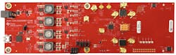
2. Supporting the ADC, the ADC12DJ5200RFEVM is an RF-sampling ADC evaluation module (shown without heat sink).
The TSW14J57 is a next-generation data-capture card. Populated with an Arria 10 device and using the Altera JESD204B IP solution, it can be dynamically configured to support all lane speeds from 1.6 to 15 Gb/s across 1 to 16 lanes (Fig. 3).
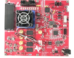
3. Additional support is available using the TSW14J57EVM Data Capture/Pattern Generator evaluation module with 16 JESD204B lanes from 1.6 to 15 Gb/s.
For more-ambitious designs, TI offers the TIDA-010128, a scalable, 20.8-Gsample/s, 12-bit reference design (board is not for sale) that leverages the aperture-delay adjustment feature on the ADC12DJ5200RF to ease the multichannel interleaved implementation (Fig. 4). This reference design uses an on-board, low-noise JESD204B clock generator based on LMK04828 and LMX2594 to meet 12-bit system performance requirement.
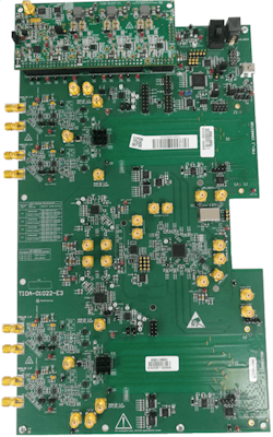
4. The TIDA-010128 reference design uses the aperture-delay adjustment feature of the ADC12DJ5200RF (with a 19-fs resolution phase-control steps) to achieve an interleaved 20.8-Gsample/s sampling rate.

About the Author

Bill Schweber
Contributing Editor
Bill Schweber is an electronics engineer who has written three textbooks on electronic communications systems, as well as hundreds of technical articles, opinion columns, and product features. In past roles, he worked as a technical website manager for multiple topic-specific sites for EE Times, as well as both the Executive Editor and Analog Editor at EDN.
At Analog Devices Inc., Bill was in marketing communications (public relations). As a result, he has been on both sides of the technical PR function, presenting company products, stories, and messages to the media and also as the recipient of these.
Prior to the MarCom role at Analog, Bill was associate editor of their respected technical journal and worked in their product marketing and applications engineering groups. Before those roles, he was at Instron Corp., doing hands-on analog- and power-circuit design and systems integration for materials-testing machine controls.
Bill has an MSEE (Univ. of Mass) and BSEE (Columbia Univ.), is a Registered Professional Engineer, and holds an Advanced Class amateur radio license. He has also planned, written, and presented online courses on a variety of engineering topics, including MOSFET basics, ADC selection, and driving LEDs.
Comment About the Article
To join the conversation, and become an exclusive member of Electronic Design, create an account today!

Leaders relevant to this article: