Microcontroller Efficiently Converts Sensor Voltage to Current
Download this article in PDF format.
When taking measurements from analog sensors located at long distances, voltage drops and noise can affect precision of the readings. Therefore, a voltage-to-current (V/I) module is needed to transmit a current in order to obtain accurate readings. The reason is well-known: According to Kirchhoff’s current law (KCL), the sum of currents entering a node must be equal to the current leaving that node; thus, the sensor’s cable length is irrelevant when transmitting current and further, the low impedance of a current loop minimizes noise pickup in contrast to a voltage signal.
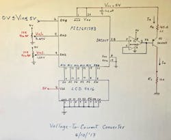
1. This circuit, based on a PIC microcontroller with a few added components, converts a sensor-based voltage into a 4- to 20-mA current loop. Shown is the circuit as originally drawn on a whiteboard.
The circuit in Figure 1 will deliver an output current from 4 to 20 mA for an input voltage (Vin) from 0 to 5 V. PNP transistor Q1 (2N2907) is configured as a constant-current source; its emitter current and resistor value (Re) are defined by the equation:

where Vcc = 5 V, and Vbe = 0.7 V.
Transistor base voltage Vb must be within the range of 3.64 V to 1.00 V to control the emitter current from 4 to 20 mA. Thus, a 165-Ω resistor is the appropriate value to generate that current loop. Since Vb will be generated within that range, a PIC microcontroller is selected to control the transistor’s base voltage. A microcontroller that suits these needs is the PIC16F1783, because it has both analog-to-digital and digital-to-analog converters (ADCs and DACs).
The ADC input will be reading the sensor’s input voltage on channel AN0, and with some processing, it will then control the voltage output in the DAC module. An op amp (MCP602) is configured as a driver and used to buffer the DAC’s analog output. The 8-bit DAC will provide a voltage output with a resolution of 20 mV, while the 10-bit ADC has a resolution of 4.88 mV. Therefore, the ADC reading is divided by 4 to make it compatible, and the output voltage will be controlled by the sensor’s input voltage.
The DAC voltage references are set to VRef+ = 3.64 V and VRef− = 1 V, using a pair of multiturn trimmer potentiometers. This configuration makes the DAC output vary from 3.64 V to 1.0 V. As the DAC output voltage decreases from 3.64 V to 1 V when the sensor’s input voltage increases, the PIC micro delivers a voltage from 1 V to 3.64 V. Thus, the output voltage must be inverted, so that the ADC reading is stored in variable VOLT. The ADC’s binary reading in this variable goes from 0 to 255; knowing this, we get the equation:
DACCON1 = 255 − VOLT
where DACCON1 is the DAC output value. Thus, the output voltage when VOLT is 255 will be 3.64 V as shown by:

From the Vout equation, we see that changing the DACCON1 value will change the output voltage value. After controlling the DAC’s output voltage, this signal goes to the buffer op amp which drives the base of the Q1 to control the output current, using the 16 5Ω resistor to generate the current which varies from 4 mA when Vb = 1.00 V up to 20 mA when Vb = 3.64 V.
Programming the Microcontroller
The microcontroller’s code (see listing below) is written using the PBP3 compiler from melabs.com.

In the PIC configuration for the DAC module, 8-bit register DACCON0 is used to configure the DACOUTPUT2 and both the Vref+ and Vref- pins.
- The 7th bit, DACEN, turns on the DAC if it is cleared to “0,” while a logic “1” enables the DAC module.
- The 6th bit is “0” because it’s an unimplemented bit.
- The 5th bit, DACOE1, enables DAC output DACOUTPUT2; this bit goes to “0” to disconnect output DACOUT1.
- The 4th bit, DACOE2, enables the DACOUT2 pin; setting it to “1” enables this pin and setting a “0” value disconnects the DACOUT2 pin. In this case, we are using the DACOUT2 pin, as it is set to “1.”
- For bits 3 and 2, instruction DACPS<1:0> (embedded in the DACCON0 register) determines the use of an external Vref+, where setting a value of “10” enables the use of a FVR Buffer2 output. A value of “01” uses Vref+ while with “00” it uses the Vdd as an output range. In this case, we’re using Vref+ and therefore the value is “01.”
- Bit 1 goes to a “0” logic because it is unimplemented.
- The Zero bit, called DACNSS, is used to select the negative source Vref- ; in this case, it is set to “1” to enable the Vref- Thus, the DACCON0 register configuration will be DACCON0= %10010101.
The ADC module has three configuration registers that require specific set up. Here, we want to read an analog input signal ranging from 0 to 5 V.
- For register ADCON0, bit 7 controls the ADC Result Mode and it has two possibilities, 10-bit or 12-bit results. This design uses the 10-bit result, so the bit is set to 1.
- Bits 6 through 2 select the analog input AN0, so these bits are set 0000.
- Bit 1 is the ADC conversion status. When this bit is set, the module is processing a conversion, and when this bit is set to 0, a conversion is completed. Bit 0 is the ADC Enable bit, and it is set to 1 to enable the ADC module.
- Bit 7 of register ADCON1 is the ADC Result Format, which can be in either two’s complement or sign-magnitude format. Since we are using two’s complement, this bit is set to 1.
- Bits 6 through 4 are the ADC Conversion Clock Select bits, which are set to 111 because the clock which is supplied from a dedicated FRC oscillator is selected.
- Bit 3 isn’t implemented and is set to 0. Bit 2 controls the Vref− setup; as it is connected to Vss, it is set to 0. Bits 1 and 0 control Vref+, which in this case is set to 00 to connect Vref+ to Vdd.
- For Register ADCON2, bits 7 through 4 are the Auto-conversion Trigger Source Selection bits, which must be disabled; therefore, these bits are set to 0000.
- Bits 3 through 0 are the Negative Differential Input Channel Select bits, here set to 1111 for the ADC Negative reference, controlled by ADNREF.
- Finally, the setup registers are ADCON0= %10000001, ADCON1= %11110000, ADCON2= %00001111.
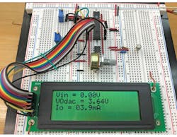
2. The circuit was built on a prototyping board with an LCD readout for convenience. The two small blue rectangles in the upper left are the trimming potentiometers used to adjust the positive and negative reference voltages.
Figure 2 depicts the circuit assembled on a prototyping board. It includes an LCD readout to show the key variables such as input voltage, DAC output, and 20-mA loop current.

About the Author
Ricardo Jimenez
Ricardo Jimenez holds a master's degree in electronics from the Instituto Tecnologico de Mexicali.
Jorge L. Aguirre
Jorge L. Aguirre is in his 4th year at Instituto Tecnologico de Mexicali, pursuing a degree in Electronics Engineering.
Thomas F. Murrieta
Thomas F. Murrieta is in his 4th year at Instituto Tecnologico de Mexicali, pursuing a degree in Electronics Engineering.
Comment About the Article
To join the conversation, and become an exclusive member of Electronic Design, create an account today!

Leaders relevant to this article: