Precision Op Amps Yield High-Accuracy Circuits
Download this article in PDF format.
The ordinary modern IC op amp is fully applicable to most standard amplifier configurations. Error sources are small and may be of no concern, or one can easily compensate for them. Yet there are some types of circuits where inherent but small op-amp error sources can’t be tolerated. As a result, precision IC op amps have been created to address these needs. Three examples here illustrate some common problems and solutions.
Sponsored Resources:
- Zero-drift Amplifiers: Features and Benefits
- Attenuator Amplifier Design to Maximize the Input Voltage of Differential ADCs
- MUX-Friendly Precision Operational Amplifiers
Zero-Drift Amplifiers
A zero-drift amplifier is one whose output doesn’t change significantly as a result of the amplification of negative physical characteristics like input offset voltage. Op amps are high-gain dc differential amplifiers that commonly have mismatched input components and device limitations that introduce error signals.
The most common and detrimental error is input offset voltage. This characteristic is caused by small differences in the input differential transistors’ or any related resistors. This error is usually very small, and in many applications, it can be ignored as it doesn’t cause any detrimental effects. However, in applications where very small input signals are to be amplified with very high gain, this unwanted error voltage is amplified along with the desired input. The output, therefore, isn’t representative of the true input.
In addition, the input offset voltage error varies with temperature, introducing further obfuscations of the true signal. This drift is usually stated in microvolts per degree Celsius (µV/°C).
This problem has been known for decades. In applications that can’t tolerate such errors and drift, compensation methods have been devised. Most older and a few current IC op amps have a separate null or trim pin input to which a corrective voltage can be applied. Another solution is to add a resistor in the non-inverting input, which will correct for bias current variations. These methods don’t correct the drift, though. Precision op amps are available to solve these problems.
Zero-drift amplifiers feature an input offset voltage of less than a microvolt. Drift is reduced to fractions of a nanovolt (nV) variation per °C. Some of their key features include CMOS semiconductor technology, rail-to-rail input and output, and the use of chopping techniques.
The term rail-to-rail refers to the ability of an op amp to achieve an output or input that can vary over the full range of the dc supply voltages. This feature is realized with CMOS circuits. For instance, if an op amp uses ±5-V supplies, the output can swing over the full range from – 5 V to + 5 V or 10 V. For a single-supply op amp, the range would be 0 to + 5 V. The actual output limits would be within about 10 mV of the supply limits. This definition also applies to the input-voltage range.
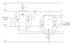
1. This complementary pair input arrangement permits CMOS op amps to handle rail-to-rail input signals.
To achieve the rail-to-rail feature, the zero-drift amplifiers use the input arrangement shown in Figure 1. The differential input signal is applied simultaneously to both the PMOS and NMOS pairs. The NMOS devices deal with input signals in the (VDD – 1.8 V) to VDD range, while the PMOS pair handles the voltages from VSS to (VDD − 1.8 V). As the input signals transition from one range to another, they introduce a form of crossover distortion. This distortion is removed by internal correction circuitry (discussed later).
Another way to achieve the rail-to-rail input range is to use a single input differential pair with an internal charge pump. The charge pump increases the input amplifier voltage by about 1.8 V above VDD. This eliminates the crossover distortion.
The low offset and zero-drift characteristic is sometimes achieved by laser or other trimming of the input components during manufacturing. Most newer precision amplifiers use an internal correction technique known as chopping to realize the zero-drift characteristic. Also known as auto-zero amplifiers, these devices employ internal switching circuits that “sample” the offset and cancel it out.
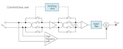
Figure 2 shows one of several possible configurations. The input is applied simultaneously to a conventional amplifier and a nulling amplifier (upper path in the figure). The nulling amplifier looks at the input offset of the standard amplifier. In the first phase of the switching cycle, the offset is amplified and stored on capacitor CC. In the second phase of the switching cycle, the signal’s polarity is reversed so that the earlier charge is effectively cancelled.
2. The generalized precision chopper amplifier produces near-zero offset and virtually no drift or 1/f noise.
The continuous charging and discharging produces an average output across CC of zero. The switching occurs at a frequency usually in the 1- to 50-kHz range. This creates some transients—these are removed with a synchronous notch filter before arriving at the corrected output.
The overall result is an offset voltage of typically less than a microvolt and a drift specification of a fraction of a µV/°C. The whole process also eliminates the crossover distortion and the usual ever-present 1/f noise that occurs in op amps at low frequencies.
Zero-Drift Applications
Any application that involves the amplification of very low signal levels is a candidate for zero-drift amplifiers, because any significant input offset voltage will introduce errors. Some of the primary applications include bridge amplifiers using strain gauges or other sensors, current shunt measurement, thermocouples, IR sensors, electronic scales (load cells), and medical instrumentation. Other uses are ADC input buffer amplifiers and DAC output amplifiers.
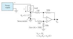
Figure 3 shows how current is determined by measuring the voltage across a 0.1-Ω sense resistor (Rs). A current of 1 A will produce a voltage drop of 100 mV, but a current of 1 mA will only produce a voltage of 100 µV. Significant amplification is needed to achieve a usable output measurement. Any major input offset voltage will introduce a huge error.
3. A precision zero-drift op amp provides an accurate amplification of voltage and the determination of current in a sense resistor.
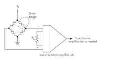
Figure 4 shows an instrumentation amplifier (IA) made up of three zero-drift precision op amps used as bridge amplifier with a strain gauge. Tiny variations in strain-gauge resistance with applied force translate into very small voltages (µV) that must be amplified to be properly measured. Rg sets the IA gain, but additional gain may be obtained with another precision amp in the signal path if needed. Zero-drift IAs ensure that op-amp errors are minimal and the outputs are accurate. The link referenced below provides more details on the zero-drift methods and circuits.
4. Bridge measurement circuits with selected resistive sensors produce tiny voltage output variations that require significant amplification to produce a useful output. A precision zero-drift op amp serves that purpose.
Attenuator Amp Design Maximizes Input Voltage of Differential ADCs
While most op-amp designs feature gain, there are some special applications where an attenuation factor is required. An example is in industrial applications where the output of a sensor or other input is greater than the maximum allowed by an ADC. An attenuator amplifier can meet that requirement. Since most ADC inputs are differential, a fully differential amplifier (FDA) with both differential inputs and outputs is needed.
Figure 5 shows a typical arrangement. The fully differential amplifier outputs drive the ADC. A follower op amp provides a high input impedance for the input source. The input is single-ended.
5. This precision op amp is used as an attenuator and buffer for an ADC.
The gain (or attenuation factor in this case) is a function of the differential amplifier resistors.
Gain (attenuation) = Vodiff/Vi = Rf/Rg
Making Rf smaller than Rg provides attenuation with amplifier buffering to the ADC. The maximum input to the ADC is usually the reference value, for example 5 V. The following reference provide more details on the challenges that engineers face when attenuating large signals for digitization and maximizing the input voltage to differential input ADCs.
MUX-Friendly Precision Op Amps
Another application that often requires a precision op-amp solution is a multichannel data-acquisition system using multiplexers (MUX). The typical data-acquisition system employs a single ADC that serves multiple inputs. A multiplexer selects the desired input for conversion. One common arrangement uses a precision op amp at the output of the MUX to drive the ADC.
Figure 6 shows the arrangement. The protection diodes are usually necessary to prevent damage caused by differential voltages higher than the amplifier’s maximum rating. This could occur when switching from one channel to another with extreme voltages and/or polarity differences.
6. Here, a precision op amp buffers the output of a multiplexer to an ADC in a data-acquisition system.
Since multiplexers switch very fast (nanoseconds) when changing input channels, the buffering amplifier must be able to keep up. Critical specifications include a fast slew rate and a fast settling time. Both JFET and CMOS precision op amps can be used. Some of the newer devices also have the protection diodes or their equivalent integrated into the IC.
Sponsored Resources:
About the Author

Lou Frenzel
Technical Contributing Editor
Lou Frenzel is a Contributing Technology Editor for Electronic Design Magazine where he writes articles and the blog Communique and other online material on the wireless, networking, and communications sectors. Lou interviews executives and engineers, attends conferences, and researches multiple areas. Lou has been writing in some capacity for ED since 2000.
Lou has 25+ years experience in the electronics industry as an engineer and manager. He has held VP level positions with Heathkit, McGraw Hill, and has 9 years of college teaching experience. Lou holds a bachelor’s degree from the University of Houston and a master’s degree from the University of Maryland. He is author of 28 books on computer and electronic subjects and lives in Bulverde, TX with his wife Joan. His website is www.loufrenzel.com.
Voice Your Opinion!
To join the conversation, and become an exclusive member of Electronic Design, create an account today!

Leaders relevant to this article:


