Take a Flier on the Flyback for Your High-Voltage Circuit Design

Download this article in PDF format.
Applications ranging from consumer electronics to high-power energy-conversion systems leverage the benefits of dc-dc power converters in their designs. Among these, flyback converters are popular for low-power applications such as backlighting for LCD monitors and TVs, micropumps (i.e., microbiological experiments), piezoelectronics, and Geiger counter tubes. This kind of flyback converter is highly scalable and reusable for applications ranging from 30 V to 450 V by simply varying configuration parameters of a Silego GreenPAK programmable device, a configurable mixed-signal IC (CMIC).
For instance, high-voltage LEDs offer the optimum solution for indoor retrofit lamps. High-voltage LEDs usually have a higher turn-on voltage, greater than 20 V, than conventional LEDs (white LEDs), which is typically 3 V. This low-current, high-voltage architecture enables simpler, smaller, cheaper, and higher-efficiency driver topologies. A high-voltage, low-current LED string matches the LED output voltage more closely to its ac input voltage versus that of a low-voltage, high-current string using the same number of LEDs and lumen output.
For LCD backlight lamps, the LEDs are on the edge of the display, and a light-guide plate helps achieve uniform backlighting (Fig. 1). White LEDs usually employ a constant-current drive using pulse-width modulation (PWM) for dimming control. You can drive the LEDs in series through the flyback converter in order to produce enough voltage to illuminate a large LED string. Along with easy control, series connections also simplify pc-board routing and enable optimum current matching between LEDs. Therefore, series connection is the preferred approach.

1. Display monitor structure: The LEDs on the edge of the display and a light-guide plate aids in achieving uniform backlighting. LEDs can be driven in series through the flyback converter to produce enough voltage to illuminate a large LED string.
For medical or biological devices used in precision, controlled liquid delivery, such as infusion pumps, insulin pumps, or nebulizers, piezoelectric micropumps offer an attractive alternative to standard pumps. Piezoelectric micropumps are small, lightweight, low power, low cost, and accurate (Fig. 2). These miniaturized mechanical pumping devices employ a piezoelectric actuator in combination with passive check valves. When voltage is applied, a piezoelectric actuator expands or contracts, which causes the liquid or gas to be sucked into or expelled from the pump chamber. The check valves on both sides of the pump chamber govern the flow in one direction.
Flyback converters benefit from galvanic insulation, multiple input and/or output stages, compactness, and simple construction. Their key component is the high-frequency transformer. This article offers a detailed explanation of the dc-dc flyback converter using Silego technology—one that can dynamically control the output voltage.
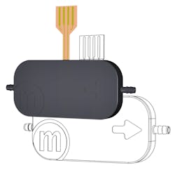
2. 250-V micropump: A miniature, slim, and lightweight micropump driven by piezoelectric element. The driving voltage and frequency for operating the piezoelectric micropump can be arbitrarily set by an external control signal, which enables a flow rate control.
The GreenPAK offers a new point of view in application development by merging analog and digital configurable blocks. The main advantages are miniaturization, flexibility of multiple configurations, and simple programming (GreenPAK Designer). Complex circuits can be realized by mixing analog and digital elements, and there’s no need for another programming language.
In this application example, we will show how the Silego GreenPAK can be used to:
- Read the analog output voltage for feedback control.
- Compare read voltage with a fixed value chosen to deliver the exact output voltage.
- Perform pulse width modulation in order to drive the power MOSFET.
- Deliver precise operation sequencing through the internal oscillator.
Flyback Operating Principles and Model
The basic topology of a flyback circuit is shown in Figure 3. When a MOSFET is switched ON and a voltage is applied to the primary winding, the primary current rises linearly. The change of input current is determined by the input voltage, the transformer primary inductance, and the on time. During this time, the energy is stored in the core of the transformer, the output Diode D1 is reverse-biased due to the voltage induced by the primary, and the energy isn’t transferred to the output load.
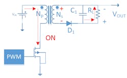
3. Flyback circuit ON phase: The MOSFET is switched on and a voltage is applied on the primary winding through the transistor. Energy is stored in the transformer’s core and the output Diode D1 is reverse-biased, due to the voltage induced by the primary. Energy isn’t transferred to the output load.
The current in the primary rises linearly:
I = (VIN/L1)t
And the voltage in the secondary is:
VSEC = NSVIN
So the reverse voltage of the diode should be at least:
VREV = NSVIN + VOUT
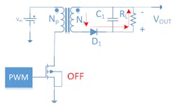
4. Flyback circuit OFF phase: The MOSFET is switched off and the primary remain open. The voltage induced in the secondary can charge the output capacitor and source the load.
When the MOSFET switches off (Fig. 4), the energy accumulated in the primary is:
E = (1/2)LI2
Due the fact the primary is opened, the voltage is induced in the secondary and the diode is forward-biased. The current is fixed by the transformer ratio n = NS/Np:
IS = Ip/n
and the voltage:
VS = VOUT + VD
If the voltage drops across the switching MOSFET and the output rectification diode are ignored, the voltage during the on time (TON) should be equal to the voltage during the off time (TOFF), in steady-state operation:
VINTON = VOUT(Np/NS)TOFF
If we define D as the duty cycle:
D = [TON/(TON +TOFF)]
We can obtain the relationship between turn ratio and input voltage to the output voltage:
VOUT ≈ VIN[DMAX/(1 ‒ DMAX)](NS/Np)
The increase of maximum duty cycle reduces the peak current in the primary of the transformer, resulting in better transformer utilization in the primary, and lower ripple on the input source. At the same time, the increase of the maximum duty cycle increases the maximum stress voltage between drain to source of the main switching MOSFET, and increases the peak current on the secondary side.
A flyback converter has two different modes of operation: discontinuous mode and continuous mode. In the discontinuous mode, all of the energy stored in the primary during the on time is completely delivered to the secondary and to the load before the next cycle. There’s also a dead time between the instant the secondary current reaches zero and the start of the next cycle. In continuous mode, still some energy is left in the secondary at the beginning of the next cycle. The flyback can operate in both modes, but it has different characteristics.
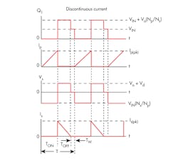
5. Discontinous current mode: The energy stored in the primary during the on time is completely delivered to the secondary. Higher peak currents and higher output-voltage spikes occur during the turn-off.
The discontinuous mode has higher peak currents, and therefore higher output voltage spikes during the turn-off (Fig. 5). On the other hand, it maintains faster load transient response and lower primary inductance, which means the transformer can be smaller in size. The reverse-recovery time of the diode isn’t critical because the forward current is zero before the reverse voltage is applied. Conducted EMI noise is reduced in discontinuous mode because transistor turn-on occurs with zero drain current.
The continuous mode has lower peak currents and, therefore, lower output voltage spikes (Fig. 6). Unfortunately, it makes the control loop more complicated because of its right-half-plane (RHP) zero that forces a reduction in the overall bandwidth of the converter.
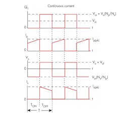
6. Continuous current mode: Lower peak currents and voltage spikes occur, but a more accurate control is required.
Flyback Circuit Design and Simulation
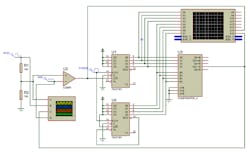
A simulation in PSpice was performed to verify the circuit design. A transformer with turn ratio 1:10 was chosen with an input voltage of 5 V. R1 and C3 components form a snubber network to protect the MOS1 transistor from high voltage spikes.
Si7898DP is a high-voltage N-channel MOSFET with 150-V maximum drain voltage and low drain-source resistance (RDS-ON0.095 @ ID = 3 A and VGS = 6 V) (Fig. 7). The diode has been chosen with high speed (reverse recovery < 4 ns) and high peak reverse voltage (100 V). The two capacitors are suited for high voltage applications with a maximum voltage rate of 1000 V.
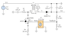
7. Flyback circuit schematic: T1 is a 1:10 transformer, and R1-C3 forms a snubber circuit to avoid peak voltage on the transistor.The PWM and the feedback is simulated with a voltage-controlled oscillator, which outputs a signal whose frequency is proportional to the feedback voltage. The high voltage on the secondary is fed back thorugh the voltage divider R3-R2. The capacitors C1 and C2 sustain the voltage in the ON phase.
The PWM signal that drives the MOSFET is simulated by a voltage controlled oscillator (VCO-Sqr) and generated by the Silego GreenPAK. The control signal is the voltage on the resistor divider R2, which acts as feedback of the output.
In the first graph (red line) of Figure 8, the feedback voltage scaled by the divider is sent to the pulse-width modulator. By this, the voltage controlled oscillator (VCO) sets the duty cycle to the MOSFET (green line in the third graph). As shown, the duty cycle and the frequency decreases when the voltage goal is reached.
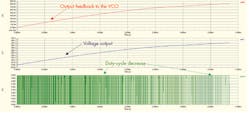
8. Simulation output plots: The first plot (red line) shows the output feedback to the VCO. The second plot (blue line) represents the output voltage. With the increase of the output feedback, there’s a proportional increase of the output. In the third plot (green line), the increase of feedback produces a reduction of the duty cycle.
The VCO generates a square wave (green line, Fig. 9) of 200 kHz, and at every falling edge, the energy stored in the transformer is delivered to the load, increasing the output voltage. The voltage increase in the load is reflected on the primary and attenuated by the RC snubber network.
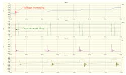
9. Enlarged graph simulation: When the voltage in the PWM drops, the voltage on the MOSFET drain increases (purple line) and the diode is reverse-biased (yellow line).
GreenPAK Design
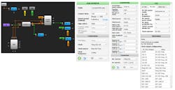
The GreenPAK SLG46620Vis at the heart of the flyback converter (Fig. 10). It converts the output voltage from the divider to a pulse-width modulation in which the duty cycle varies to obtain the prefixed output voltage. When the output voltage is lower than a prefixed threshold, the duty cycle is maximized to reach that voltage. Subsequently, the duty cycle decreases and the output voltage becomes stable. Our purpose is to arrive at 450 V—it’s for this reason an external power supply was used through an USB connection.
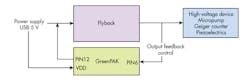
10. Flyback system design: Here, the power-supply unit goes through a USB, e.g., the GreenPAK acts as an output feedback controller and PWM.
The voltage at GreenPAK 4 SLG46620V on pin 6 (Fig. 11) is the output feedback control, which is compared through the ACMP0 to the DAC0 output. This value is set as the goal voltage to reach by the output:
VOUT[R3/(R3 + R2)] = 450 V[(18 kΩ/(18 kΩ + 10 MΩ) = 0.809
11. Silego Matrix 0 design: The feedback is connected to the pin 6 and compared between the DAC0 fixed reference. When comparator’s signal goes down, the counter is activated, incrementing the counter.
And the digital-to-analog converter (DAC) register is set at 206, which means:
VREFDAC * (206/255) = 1 V(206/255) = 0.808
In this way, when the voltage at input pin 6 is lower than the DAC output value, the analog comparator goes down, and through INV0 the counter is up counting.
The CNT8 is set initially to 255 (Fig. 12). The difference between the two signals is always positive and duty cycle is at maximum (99.6%) in order to obtain the desired output voltage value. When the voltage reaches 0.808 V, the ACMP goes low, INV0 goes high, the counter is down counting, and the duty cycle decreases.
12. Silego Matrix 1 design: The value of counter 2 is passed to CNT8, which is set initially to 255. The difference between the two signals is always positive and duty cycle is at maximum (99.6%).
To set a different voltage, exactly the same configuration can be maintained; only a software change is required. By following the previous equation for 250 V and 100 V, we can obtain:
VOUT250V[R3/(R3 + R2)] = 250 V[18 kΩ/(18 kΩ + 10 MΩ) = 0.449
And the DAC register should be set, through the following equation, at 115:
VREFDAC * (NSTEP/255) = 0.449 => 1 V(NSTEP/255) = 0.449 => NSTEP = 0.449 V * (255/1 V) = 115
In the same way for 100 V, we obtain:
VREFDAC * (NSTEP/255) = 0.180 => 1 V(NSTEP/255) = 0.180 => NSTEP = 0.180 V * (255/1 V) = 46
GreenPAK Simulation and Validation
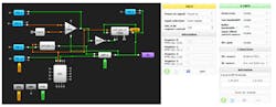
The PWM generator of the flyback circuit was simulated using Proteus simulation suite. Fig. 13 shows the digital simulation diagram of the PWM generation section. Starting from the left, two resistors simulate the voltage divider at the flyback output stage. The divider input was simulated with a sinusoidal generator having approximately 5 V dc offset. This means that the IN+ of the comparator is at 2.5 V with an ac-coupled sinusoid of 200 mV p-p. The sinusoid variations around the dc value simulate the variation of the high-voltage output around the setpoint of 450 V. A fixed voltage reference of 2.5 V is connected to the inverting input of the comparator. The constant voltage simulates the output of the Silego GreenPAK DAC.
13. PWM digital simulation is possible thanks to Proteus. The comparator enables two counters that control the duty cycle.
The discrete counter U4 simulates the Silego GreenPAK ramp generator (i.e. CNT8/DLY8). It’s a free running counter starting from the maximum value toward the zero value. In fact, due to the connection of the pin D/Ū to the high level, is in down counter mode. The counter U1 is in free running mode too. In this case the D/Ū input is controlled by the comparator output voltage level.
U1 counter is in DOWN mode. Vice versa, when IN->IN+, the analog comparator output is low and U1 counter is in UP mode. The output of the two counters are digitally compared through a digital comparator U3. The output was kept on the A>=B pin of the digital comparator. For the sake of simplicity, the simulation was performed by considering 4-bit counters and a digital comparator. One digital oscilloscope is used to show the signals during the simulation. Channel A monitors the resistor divider output, channel B the resistor divider input, channel C the PWM output, and channel D the voltage reference at the DAC output. Besides the oscillator, a logic analyzer shows the counter outputs, the analog comparator output, and the digital PWM output.
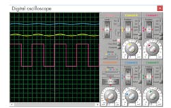
14. Analog input stage simulation: Channel A monitors the resistor divider output (yellow line), channel B the resistor divider input (blue line), channel C the PWM output (purple line), and channel D the voltage reference at the DAC output (green line).
Looking at Figure 14, the C trace (PWM output) was exchanged with the analog comparator output. The blue trace is the input voltage at the resistor divider. The green trace is the DAC reference voltage output (IN+), while the yellow one is the voltage at the middle of the voltage divider (IN‒). As you can see, when the yellow trace is above the reference voltage, the comparator output goes high, while the opposite is true when the yellow trace is below the green one. The comparator output is represented by the pink trace.
Figure 15 shows the digital comparator outputs (channels A0-A7), the analog comparator level (channel A14), and the PWM digital output (channel A15). The clock signal is fed at lower frequency than the real application circuit to improve the signal’s visibility and understanding. What’s worth noticing is that when the analog comparator is at the high-voltage level, the PWM is relaxed; the opposite is true when the PWM signal is at widest. Focusing on the high-level case, the flyback high-voltage output is increasing, which means the PWM signal must be relaxed. This leads the flyback output toward the setpoint value.
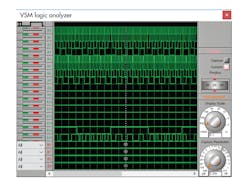
15. Logic analyzer signals: Two output counters are linked to the logic analyzer and plotted. A15 is the effective output signal of the PWM.
The main features of this architecture are:
- A minimum PWM signal is always guaranteed.
- No synchronization is needed between the Silego blocks.
- Around the setpoint value, output tracking is performed digitally.
GreenPAK Application Circuit and Testing
Figure 16 shows the real circuit assembled on a breadboard, with the Silego development board on the left and the flyback circuit on the right. The internal 5-V regulator supplies the Silego development board, while a USB 5-V hub supplies the flyback circuit. This choice was adopted to avoid a huge load on the internal regulator of the Silego GreenPAK. The ground reference is the same for both.
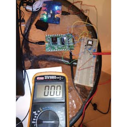
16. Application circuit and testing: On the top, a USB hub powers Silego’s chip and the dev board. A multimeter is connected to the output for monitoring the voltage’s rise.
Figure 17 shows the Silego programming interface. As you can see, the internal regulator is used, while the analog comparator input (TP6), the PWM signal output (TP12), and the GND signal are routed on the expansion connector.

17. Silego programming interface: It provides the ability to enable the LEDs on the boards, pull the outputs up or down, and simulate buttons. In addition, a signal generator can simulate external signals.
The connections were realized with rigid wire cable and female standard headers. The TP12 pin is connected to gate of the MOSFET, while the middle point of the resistor divider is connected to the TP6 pin. The reset/delay input TP2 was simulated with a button in non-latched mode configuration. As you can see, the EC flag is selected on the TP6 and TP12, enabling the external connection. A digital tester is connected on the flyback output with a full scale of 1000 V. We expect an output voltage of approximately 450 V. The multimeter measurement is shown in Fig. 18.
The circuit starts running by pressing the Testing/Emulation mode button. The reset button (TP2) is fixed to the logical high level (5 V). Before you start running the flyback, please take care that all of the connections are right; don’t touch any parts during high-voltage generation. When the circuit is supplied, you can see the voltage increasing on the digital multimeter display. The voltage increase is very fast, reaching the setpoint value of 450 V in a few seconds. The value remains stable around the setpoint value until you disable the emulation mode by clicking on the Emulation button. When the Silego development board is switched off, the output goes to zero in a short time.
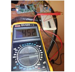
18. The voltage multimeter monitors the flyback output voltage when the setpoint is reached.
Please be sure that the voltage on the multimeter is null before handling the flyback circuit.
Voltages above 400 V are usually used in the Geiger counter application. Further development could involve connecting a Geiger tube to the flyback circuit for radiation particles detection. This discharges due to particle stricks, would able to be observed and counted. This was not connected because it requires a stable printed circuit board (PCB). Lower voltages between 100 V and 250 V are usually useful to drive piezo-electric devices like micropumps and MEMS devices. The output voltage can be changed by setting the right value in the DAC register input.
If the DAC full-scale value is at 1 V, with 8 bits of resolution, we have one LSB value of:
LSB = 1/(28 ‒1) = (1/255) ≅ 3.92 mV
With a resistor divider composed by 10 MΩ and 18 kΩ, and the flyback output voltage is at 450 V, the middle point of the resistor divider will be:
VDIV = 450[18k/(10M + 18k)] ≅ 808 mV
Finally, the DAC input register value is:
DACREG = (808/3.92) = 206
Conclusion
The goal of this application note is to provide a starting point on high-voltage unit circuit design. The flyback-unit configuration is the best way to achieve high-voltage values, supported by GreenPAK technology.
A typical application with a voltage of approx. 450 V is the Geiger counter. A Geiger tube can be connected on the flyback output, and with slight modifications to the base circuits, radiation particles can be detected and counted. Furthermore, a display or a PC interface can be implemented to show parameters through a Labview GUI or a TFT display unit. The added value here is the GreenPAK technology helps simplify project development in both the analog and mixed-signal fields.
About the Author
Michele Marino
Analog & Mixed-Signal Designer
Michele Marino received a Master’s in electronic engineering at “La Sapienza” University in Roma. Presently he’s working as Analog & Mixed Signal designer at LoMi Electronics.
Lorenzo Massari
Mixed-Signal and LabView Developer
Lorenzo Massari received a Master’s in digital electronics engineering. Presently he’s working as Mixed-Signal and LabView developer at LoMi Electronics.
Comment About the Article
To join the conversation, and become an exclusive member of Electronic Design, create an account today!

Leaders relevant to this article: