Understand, Measure, And Optimize Clock Distribution Additive Jitter To Achieve Best Performance
High-speed communications require system designers to optimize clocking performance while adhering to both performance and cost-budget requirements. When selecting an optimal clock, the developer must consider factors such as performance, cost, size, and output logic. But the focus is on phase noise for those who work in the frequency domain, or on jitter, which is the time domain equivalent. The selected clock often needs to be distributed to a variety of logic inputs and locations on a printed-circuit board (PCB) design.
This file type includes high resolution graphics and schematics when applicapable.
Related Articles
- Quell Those Jitters Caused By Tough Jitter Requirements
- Clocking Solutions Turn To Sub-Picosecond Jitter Performance
- Optimal Jitter Attenuation Starts With The Proper PLL Bandwidth
Great effort is spent optimizing clock performance. The clock buffer becomes part of the equation when determining overall system performance. The impact on phase noise and jitter also becomes part of the equation. To meet design specifications, the engineer must understand how to measure a clock buffer’s phase noise, what can affect its performance, and what details must be considered when comparing and selecting various clock options using the manufacturer’s published data sheets.
A clock distribution IC does not generate a clock. Rather, it regenerates and provides multiple copies. Therefore, phase noise cannot be measured unless an input is applied. The term most commonly used to quantify the quality of a clock distribution IC is “additive phase noise.” What becomes a little less common is a standard methodology for measuring additive phase jitter.
For Example
In the examples that follow, a Silicon Labs Si53311 clock buffer is used to demonstrate a recommended method of characterizing additive phase jitter and various factors that influence a typical buffer’s performance. The same principles and test methods can be applied to analyze the performance of most buffers, dividers, and other distribution ICs. It’s important to understand the dependence of additive jitter performance on input rise and fall time at a given amplitude or slew rate, output format, output frequency, and power supply voltage.
The input rise and fall times appear to have a significant impact on additive phase jitter. While this is true at first glance, what makes the equation more complete is considering both rise and fall time and amplitude or, better yet, amplitude versus rise and fall time, which is expressed as Volts/ns, or slew rate.
Most engineers will associate slew rate with analog components, such as op amps, and it’s uncommon to see a slew rate value in a data sheet for a digital component. Yet even though it’s uncommon to use slew rate, it’s a more accurate way to describe what can really improve or degrade additive phase jitter. An estimated slew rate can be calculated from the data sheet specifications if a value is not provided.
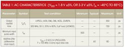
Take a low-voltage differential signal (LVDS) that has a 350-mV single-ended amplitude and a 400-ps rise and fall time. Measured at 20% and 80%, the differential slew rate would be (2 * 350 mV * 0.6)/(400 ps) or 1.05 V/ns. (The examples that follow use the differential slew rate.) Again, phase noise cannot be measured unless an input is applied and total jitter is measured. The clock buffer’s contribution is called the additive phase jitter (Table 1).
Slew rate, output frequency, logic format, and operating voltage all have an effect on additive jitter. To make a valid comparison when comparing additive jitter, similar conditions must be used, or incorrect conclusions can be reached. In a worst-case scenario, if a system designer might expect to meet a specification but the clock buffer were used in a less optimistic condition, the circuit might fail to meet requirements.
Test Examples
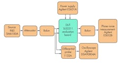
To illustrate how additive phase noise might be characterized, consider the test results below. The device under test (DUT) was a Silicon Laboratories Si53311 on its evaluation board (Fig. 1). For each test result, the slew rate was adjusted and phase noise data captured.
While slew rate can be varied easily by adjusting the signal generator output amplitude, the phase noise will vary with output level. To avoid this, the signal generator output was held at a constant level, and a combination of attenuators was used to adjust the slew rate. Note that the source noise must be lower than the DUT, ideally with 3- to 10-dB or better phase noise.
Test Results: Phase Noise
Phase noise is key to analyzing the performance of any timing device. It is a frequency domain measurement from which jitter, the time equivalent, or phase jitter (if there is a defined offset bandwidth) can be calculated. There are many reasons for using this method. It is quick and repeatable. It requires only minimal equipment optimization adjustments. It allows an engineer to analyze specific bands of interest and enables spurious signals to be identified and potentially reduced. And, most time domain measurements do not offer sufficient resolution to measure the accurate femtosecond measurements offered by today’s high-performance timing devices.
A clock buffer’s phase noise cannot be measured unless an input is applied and total jitter is measured. The clock buffer’s contribution is called additive phase jitter. To characterize the phase jitter contribution due to the buffer, the source is measured first. Then, the combination of source plus DUT is measured. Finally, phase jitter is calculated by using:
JBuffer = √( J2Total – J2Source) (1)
A fair assumption often made by designers is that the source and buffer noise are not correlated but rather are composed of purely random jitter. When a clock buffer’s additive jitter number and source jitter number (typically given as an rms value) are provided, a root sum square value is used to calculate total jitter:
J2Total = J2Source+J2Buffer (2)
J2Buffer = J2Total – J2Source (3)
The reference clock must have phase noise 3 to 10 dB lower than the DUT to accurately characterize the buffer. Counterintuitively, lower margin is required when measuring devices with lower phase noise. Often an oven-controlled crystal oscillator (OCXO) is used as a source, but this becomes problematic or at least costly at higher frequencies and can still have limitations at close-in offsets, such as 10 Hz and 100 Hz.
Many low-phase-noise sources have single-ended outputs that may need to be translated to a differential signal. In these instances, a balun provides a good cost-effective solution with minimal concern about its noise contribution. Table 2 compares the additive phase jitter performance for the same buffer using three sources having various levels of phase noise performance.
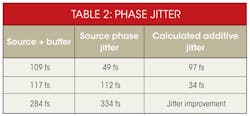
In the first example, the source has 3- to 10-dB better phase noise than the DUT. Using Equation 1 results in 97 fs of additive jitter for the buffer, which is an accurate result. However, an overly optimistic additive phase jitter number can be reported when using a source with phase noise that is similar to the buffer or DUT. The second example shows the phase noise performance for the same buffer, which is now being driven by a source with similar performance results in 34 fs of additive jitter, which is optimistic.
An extreme example of how an additive jitter number depends on the test measurement is shown in the last example, where the source has 334 fs of phase jitter, and the source plus buffer shows an improved value of 284 fs of phase jitter. Clearly, this is not a valid method of quantifying additive jitter. Care must be taken when comparing devices by using additive jitter. Another option is to check the buffer’s stated phase noise performance.
What Impacts Jitter Performance?
It is important to know what factors will affect jitter performance when a buffer is added to a clock tree. This is also very important when reading data sheets. How suppliers specify buffer jitter performance can greatly impact the number in the data sheet (Fig. 2).
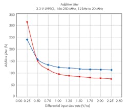
Figure 2 shows the additive phase jitter versus input slew rate for two different clock buffers. It also highlights the importance of comparing additive phase jitter using the same slew rate values and the same value that will be used in the application. In both cases, the additive jitter decreases or improves as slew rate increases. It is interesting that the results shown in red can be reported as a lower additive phase jitter solution. However, it is actually more sensitive and quickly degrades at lower slew rates, such as a low-frequency sine wave or CMOS clock.
Integration Bandwidth
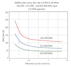
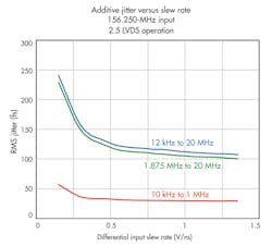
The integration bandwidth used for the jitter calculation also has a great impact on measured jitter performance. The integration bandwidth of interest will depend upon the application. If in doubt, be sure to use the same bandwidth when making comparisons. The most common bandwidth used in digital communication is 12 kHz to 20 MHz. As with most filters, using a narrower bandwidth will result in a lower and more optimistic jitter number (Fig. 3).
Output Frequency
The output frequency also has a significant impact on additive jitter. Higher frequencies will typically yield better additive jitter performance. If you know what frequency will be used, it is helpful to look at a data sheet specification that is close to it (Fig. 4).
Supply Voltage
The operating supply voltage also can affect additive jitter performance, which is an important consideration, because many clock buffers can operate from 1.8, 2.5, and 3.3 V. There was very little performance difference for the buffer family evaluated in this case, though there could be variations in additive jitter performance for another buffer family. This is an important consideration for system design and buffer selection. It would be best to either contact the buffer manufacturer or, if equipment and time are available, to characterize the performance.
The test results show how increasing the input slew rate can optimize phase noise performance. A clock buffer’s input switches at voltage, which ideally is constant but in reality has a narrow window of variation. As such, the edge timing changes due to variations in threshold, resulting in jitter degradation. A faster input slew rate spends less time in this window of variation, minimizing the impact on the system and optimizing performance.
Recommendations
The logic family, input slew rate, output frequency, and power supply voltage can affect a clock buffer’s additive phase noise. This approach helps the designer evaluate overall jitter budget requirements, simplifies device selection, and heightens awareness of the dependency upon operating conditions.
While the evaluated clock buffer was less sensitive than other available options to variations in input slew rate, optimal results will be achieved with slew rates greater than 0.6 V/ns. This is not a stringent requirement for most differential clock sources. Take, for example, an LVDS that has a minimum 250-mV single-ended amplitude and a maximum 400-ps rise and fall time at 20% and 80% of the amplitude. In this example, the differential slew rate would be (2 *250 mV * 0.6)/(400 ps) or 0.75 V/ns.
To maximize a clock buffer’s additive phase noise performance, the optimal slew rate (a 0.6-V/ns or higher input slew rate in this case) should be used, but there is no significant improvement by using costly and power-hungry ultra-fast logic. Most differential clocks (even low-output frequency options) will have sufficient slew rate.
On the other hand, low-frequency sine-wave and perhaps CMOS clocks will have slew rate limitations that will degrade overall phase noise and jitter if the edges are not sharpened. Otherwise, a designer could spend needless hours chasing down suspected power supply noise, layout issues, and other potential sources.
To maximize the input slew rate, it is best to locate the clock buffer as close to the source as possible, use a differential input that effectively doubles the slew rate and has the advantage of common-mode noise rejection, maintain a full level input swing (do not attenuate the input unless maximum levels are exceeded), and optimize impedance matching since reflections will also degrade input slew rate. It is well worth the time spent optimizing the input slew rate when designing a distribution buffer into a clock tree.
Ultimately, the designer must exercise care when evaluating clock distribution IC performance according to data sheet specifications and when designing a buffer in a circuit since variations in slew rate, output frequency and logic, integration band, power supply voltage, and test methods can produce wide differences in performance.
This file type includes high resolution graphics and schematics when applicapable.
Fran Boudreau is a senior applications engineer for timing products at Silicon Labs, where he is responsible for product support on a family of precision jitter-attenuating PLL-based ICs and low-noise clock buffers. He has been spent more than 16 years optimizing phase noise measurements on PLLs and frequency control products used in timing applications. Previously, he worked at Hittite Microwave, Vectron International, and Analog Devices. He holds a BS in electronic engineering technology from the University of Massachusetts/Lowell. He can be reached at [email protected].
About the Author
Fran Boudreau
Senior Applications Engineer for Timing Products
Fran Boudreau is a senior applications engineer for timing products at Silicon Labs, where he is responsible for product support on a family of precision jitter-attenuating PLL-based ICs and low-noise clock buffers. He has been spent more than 16 years optimizing phase noise measurements on PLLs and frequency control products used in timing applications. Previously, he worked at Hittite Microwave, Vectron International, and Analog Devices. He holds a BS in electronic engineering technology from the University of Massachusetts/Lowell. He can be reached at [email protected].
Comment About the Article
To join the conversation, and become an exclusive member of Electronic Design, create an account today!

Leaders relevant to this article: