If you have already read Jim Williams' compilation, "Analog Circuit Design: Art, Science, and Personalities,"1 then you may look on this column as a summer rerun. However, several people, after reading my 1993 comments on Frequency-to-Voltage converters, asked my opinions on Voltage-to-Frequency Converters. I realized I had written all this down already, so here is a serialized version of the chapter I wrote in Jim's book---reprinted with the kind permission of Butterworth-Heinemann, Boston, Mass. Meanwhile, I'm going hiking. ---RAP
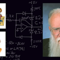
In my June 27 column, I promised to tell you all about the development of the 4701 V-to-F Converter, so here's the story. Refer to the figure for the schematic. I realized that my original circuit had depended on the power-supply magnitude for its Gain Factor. So, it had no power supply rejection, or, to be more nearly correct, it had a PSRR of about 0 dB. So I added a Zener in a bridge to create a PSRR of perhaps 45 dB. (Note, that was the first time I had ever seen such a Zener bridge----was I one of the earliest inventors of that circuit? It's a neat and useful circuit.) I also added improved features around the amplifier itself to improve the startup and the accuracy. I replaced the (sole-sourced) 805BE with the more popular and inexpensive LM301A.
I gave the breadboard to my technician, Dick Robie, to oven it and graph out the tempco from the temperature data. That night, when I was on the way out the door, I stopped and asked Dick what had he seen for the tempco. He replied, about zero. I asked, "Whaddya mean, zero. You mean, down near 100 parts per million per degree C?" He replied, "Oh, much better than 100----less than 10 ppm per degree C."
I was shocked. How could it be that good?? The next day, I figured out the fortuitous situation: For the "charge-dispensing capacitor," I had, of course, used one of the best capacitors in the house, the most precise and stable ones, which were polystyrenes with a tempco of -110 ppm/°C.
This tempco was just about cancelled out by the tempco of the entire group of diodes in the rest of the circuit. Namely, the driven end of the capacitor moves about 12.4 V p-p, plus the Vf of 4 diodes.
These 4 diodes run rich at about 6 mA, and have a tempco of about -2.0 mV/°C. The peak-to-peak voltage of these 4 diodes is approximately cancelled by that of the other four Vbes at the other end of the Polystyrene capacitor, but those diodes run at about 0.1 mA, and their tempco is about -2.3 mV/°C.
The difference of these is about 4 X 0.3 mV/°C, or 1.2 mV/°C, which is about big enough to cancel out the -110 ppm/°C of the capacitor. Now, there were several things I could have done to fix it if the tempcos hadn't come out even. For example, I could have used 3 diodes, or 5, or 4 1/2, or 3 1/2, but if 4 was the right answer, I'd go with it.
Now, how DOES this Kluge Work?? The best way for me to explain how the 4701 V-to-F Converter really works is for you to trust me, and assume that it really does work. After we analyze each section of it, then you will agree that was a reasonable assumption.
First, let's assume that the - input of op amp A1 is a few millivolts more negative than the + input, and that Vin is some positive voltage. Rather soon, the voltage at the - input will cross over and exceed that of the + input. Now, during this time, A1's output has been at the + limit, near +13 V. But when the inputs cross, the output will rapidly slew to -13 V. What are the interesting things happening then?
(1) Because there's positive feedback through C3 = 10 pF, the + input is driven a few volts negative. This ensures that there will be a good wide healthy pulse----at least 17 or 21 µs.
(2) The right-hand end of C2 is driven from about +7.5 V to -7.5 V, and the left-hand end of C2 is discharged through the emitter of Q1. That's a specific amount of charge, Q = C X ∆V. And the V isn't just the 15 V p-p at the right-hand end of C2, but rather it's that 15 V p-p minus the 2.5-V p-p excursion at the left-hand end. When this charge is driven into the emitter of Q1, it comes out of the collector (well, at least 99.5% of it does) and pulls the voltage on the 3.3-µF capacitor down by about 12 mV. During this time, the voltage at the + input of A1 is much more negative than that, so this step of -12 mV is just a minor jump. But, that charge is the magic element of precision. You see, the size of the 12-mV jump isn't important, but the amount of charge is.
Note, in most conventional V-to-F converters, the charge is dispensed by a timer circuit such as an LM555, which gates a current ON and OFF, so Q = I X T. However, you do need several precision resistors. Even then, though, the timer is subject to drift and noise, making it a rather crude, drifty, noisy, unstable kind of charge dispenser. In the 4701, the gain depends almost entirely on just 3 elements----the Zener voltage, the capacitor, and the input resistor R8. It's true that the diodes enter in, but since the Vfs of D1, D2, D3, and Q1 cancel out the Vfs of D4, D5, D6, and D7, then there's not a lot of error or drift likely there.
(3) Now that the output is staying at a negative 13 V and most of the charge on C2 has flowed through Q1, there are 2 more details going on:
(a)During this time, the current through R2 pulls at the emitter of Q1 and makes sure that Q1's emitter settles at a stable voltage. It makes sure that Q1's emitter voltage doesn't tail off to some drifty voltage. Even though R2 looks like it will dump in current that would hurt precision, it actually helps the precision. Even though a precision capacitor used in a precision VFC would normally not have a 3-MΩ resistor across it leaking like crazy----this circuit thrives on exactly that "leakage"----because it makes the emitter voltage settle to a consistent level.
(b)The voltage at pin 3 of A1 (V3) is tailing up gradually to be more positive than the voltage at pin 2 (V2). After all, pin 2 was pushed down 12 mV. Soon, after about a total of 20 µs, V3 will cross V2 and the output will bang back up to +13 V.
(4) Okay, now finally V3 crosses V2 and A1's output goes positive. We have to wait for the current through R8 to pull V2 up the 12 mV that it was pushed down. That time will, of course, depend (inversely) on the size of the signal input; the bigger, the faster. That means the time between pulses could be anything between 90 µs and 9 or 90 ms.
Are we forgetting something? Yes. The peak-to-peak voltage at the left end of C2 must be stable and constant and invariant of rep rate. But the diodes there might give a long tail----the voltage might settle gradually and give a different peak-to-peak value at different speeds. By definition, that would hurt the linearity.
What's the fix? The current through R2 is the fix. That current flows through D1, D2, and D3, and forces the left end of C2 to settle to within a millivolt or two of its final dc value in just 50 or 60 µs. Without R2, the linearity goes to pot. Now, it looks REALLY STUPID to have a circuit like this in which the "precision capacitor" C2 has a resistor across it that makes so much "leakage." But that controlled "leakage" turns out to be EXACTLY the reason for the precision and excellent linearity. The Swedish design didn't have this, and while their circuit had good linearity at 1 kHz, it couldn't be made to work well at 10 kHz. But the basic charge dispenser, when driven with suitably fast transistors, works well at 100, 1000, and even 5000 kHz.
What else is in the circuit? D8 is needed between pins 1 and 8 of the LM301A to keep it from wasting excessive current in its - limit. D9 works well to protect the + input from overdrive in the + direction. Q3 functions only when you overdrive the input----let's say, pull Vin up to +50 V----and put in so much current that the VFC stops. Then it stops with pin 2 of A1 at +1 V, and pin 6 at -13 V. It would never put out another pulse. It would never restart, even if Vin falls to a legal level, such as +1 or +5 V. However, we have added Q3. So, after a lag, C5 gets pulled minus, and Q3 turns on and pulls pin 2 so low that operation does start again. In normal operation, Q3 just sits there and does nothing, biased OFF.
C7 acts as a pulse stretcher. The pulse width at the output of A1 is about 22 µs. But we had a companion F-to-V converter, the 4702, that could only accept 20 µs (or wider) pulses. If A1's output pulse got any narrower than 20, the 4702 would lose accuracy. We solved the problem by putting in C7. Therefore, when A1 makes a 20 µs pulse, the base of Q2 would be held off a little longer than that due to the RC lag----about 15 µs extra. Then a 4701's pulse was always plenty wide enough to drive a 4702.
The little capacitor C6 was added to make the peak-to-peak voltage at V2 a little bigger. So, when some LM301's were a little slow, there was now a bigger signal between V2 and V3, and the amplifier wouldn't balk. After all, the LM301 is characterized as an operational amplifier, and if some are a little slower than others when you run them as a comparator, you really can't complain....
As you can see, the 4701 circuit did get a couple of band-aids, but not too many, and we never really did get stumped or stuck in production. Our customers loved the linearity, the tempco was pretty good, and the frequency output would never quit. The customers figured they really got their money's worth, and I certainly couldn't disagree with a satisfied customer.
I got my boss, Dave Ludwig, to approve the layout of a printed-circuit board, and I think Wayne Norwood was the guy who laid it out. We built up a few dozen and evaluated them thoroughly. I wrote up a draft of a data sheet, and I negotiated with Skip Osgood and Bill Bernardi to get it printed properly. I made up some test equipment and we got a silk screen for the module, and we called it the 4701. We were in the Voltage-to-Frequency Converter business.
To this day, I don't recall exactly how we got these V-to-F Converters to be so popular. I can't recall how we found so many customers, or how we publicized the VFCs. I asked Frank Goodenough because I knew he had been involved. He recalled that he had looked at some of the characteristics of this 4701, and he suspected that a good V-to-F Converter might be useful at The Foxboro Company, the big process-control experts. Indeed, he did find some interest there. The company was very interested, but it never bought very many because they wanted to buy only parts available from multiple sources.
The 4701 became popular, with many customers at many companies. It became profitable. It became good business. If I had all the time and space in the world, I would tell you how the 4701 led to the 4702 (a 10-kHz F-to-V Converter using the same charge-dispensing principles) and the 4703 (l00-kHz full-scale VFC) and the 4705 and 4707 (1-MHz and 5-MHz VFCs). Also, the 4709, 4711, 4721, and 4715 VFCs, and 4704, 4706, 4708, 4710, and 4722 FVCs. Some of these had a moderate tempco of 150 or 44 ppm/°C, but some were well-trimmed and guaranteed to 6 ppm/°C----as good as the best DVMs of the day.
But it all started with that crummy little 4701----and the principle that one cheap operational amplifier driving a little charge dispenser could make a very linear data converter. This came from an understanding that you could build an oscillator with a UJT and an operational amplifier to help improve the linearity, and then throw out the UJT!! I was able to do that because I was receptive to the concepts that would make a good Voltage-to-Frequency converter, even though I had never seen a Voltage-to-Frequency converter!
I was able to make accurate measurements, to throw in precision components----Zener references, capacitors, resistors----and to get inexpensive IC amplifiers, and to optimize the whole little system. What's the lesson for us to learn?
I like to think of the words of Branch Rickey, manager of the St. Louis Cardinals in the 1920s (and later manager of the Brooklyn Dodgers). One of his favorite sayings was "Good luck is the residue of design." When he referred to his baseball teams, he meant that his players were able to handle any play, field the ball, throw to the right base, etc., no matter how surprising the bounce of the ball might be.
If his players had learned the fundamentals, if they were prepared for any situation, they could take advantage of game situations and WIN. Other people might say his players were just lucky, but he knew darned well that he had trained them and drilled them so they would instinctively know to do the right thing.
I, too, was in a situation where I was prepared to take advantage of the opportunity, and I didn't drop the ball when it came my way. (Well, I fumbled it for a while but then I got it right.) That's the point of this column: When somebody hands you a gift on a silver platter, you really must be prepared to recognize it.
All for now. / Comments invited! RAP / Robert A. Pease / Engineer
Address:
Mail Stop D2597A
National Semiconductor
P.O. Box 58090
Santa Clara, CA 95052-8090
References:
1. "Analog Circuit Design: Art, Science, and Personalities," edited by Jim Williams, 1991. 398 pages. Butterworth-Heinemann, Boston, Mass., (800) 366-2665. About $51. An excellent book; you should have your librarian order it.
About the Author
Bob Pease
Bob obtained a BSEE from MIT in 1961 and was a staff scientist at National Semiconductor Corp., Santa Clara, CA, for many years. He was a well known and long time contributing editor to Electronic Design.
We also have a number of PDF eBooks by Bob that members can download from the Electronic Design Members Library.