Download this article in PDF format.
Today, cars need to do more than stop and go quickly and comfortably. With data-storage requirements no longer just driven by navigation and infotainment systems, but by advanced driver-assistance systems, or ADAS (market research firm Strategy Analytics expects that by 2021, automotive OEMs will be spending more than $37 billion per year on assistance and safety solutions), data-storage subsystems must be developed with small packages to meet space constraints and high density to handle advanced applications.
It’s also no secret that automotive makers are racing against each other to produce the first autonomous cars, relying on radar, LiDAR, cameras, night-vision devices and other sensing technologies. As we move from level 1 and 2 autonomy toward level-5 full autonomy, it’s estimated there will be between 3 and 10 GB of new data generated every second. Even a car with level-2 autonomous capabilities generates up to 1 GB of data/second.
Since you can’t transmit everything to the network or the cloud (and you don’t want to for latency reasons), massive storage is needed (Fig. 1). This will result in a possible fourfold increase in non-volatile memory (NVM) content, increasing from 16 GB to 128 GB to 64 GB to 1.0 TB, depending on the level of autonomy.
1. Autonomous-vehicle applications generate a high volume of data, which has engineers focusing on efficient storage strategies. (Sources: Strategic Analysis, Intel, 2018 Flash Memory Summit presentation)
In a self-driving car, a four-hour trip could generate more than 16 TB of data (4 TB per hour). But where will all of this data reside? Initially in local memory, as not all of it will be preserved, and what needs to be stored long term will eventually be uploaded to the cloud.
NAND in Demand
When the penetration of level-4 smart cars reaches 1%, industry watchers predict that demand for NAND will be 25X more than current requirements.
According to a recent study by Allied Market Research, the 3D NAND flash-memory market will reach $99.77 billion globally by 2025. Among types, TLC flash, the triple-level-cell segment, which accounted for more than half of the total market share in 2017, will continue its dominance, registering the fastest CAGR of 37.1% from 2018 to 2025. This is because TLC flash, which stores three bits of data per cell, offers a lower price per gigabyte as compared to SLC and MLC flash.
Put succinctly, it’s all about storage. By 2025, on-board automotive storage will exceed 1 TB, in part to help feed on-board AI for autonomous driving and traffic management. And when we consider storage, the primary medium now is 3D NAND, a technology that stacks transistors atop one another to solve speed and cost issues.
As you read this, the IEEE is just wrapping up ISSCC (International Solid-State Circuits Conference) 2019 in San Francisco. On the storage side, the world's largest international academic conference on state-of-the-art semiconductor technology is pushing 3D NAND flash memory and three- and four-bit-per-cell (TLC and QLC, respectively) programming.
Here are a couple of current state-of-the-art memory implementations discussed at ISSCC 2019:
- The industry's highest 3D memory stack with 128 layers and peripheral circuitry under the memory array, resulting in a 512-GB TLC chip delivering a write throughput of 132 Mb/s.
- A 512-GB TLC chip, while a 96-layer device using QLC pushes the density to 1.33 TB per chip or more than 1 GB per square millimeter.
This follows ISSCC 2018, where both a 1-TB, 4-bit-per-cell design achieved 5.63-mm2/GB areal density and a 512-GB, 3-bit-per-cell 3D NAND with 96 stacked word-line layers were presented.
UFS 3.0
JEDEC’s UFS (Universal Flash Storage) is a high-performance interface designed for use in applications that require minimized power consumption. The main idea behind UFS is to bring higher data-transfer speed and increased reliability to flash-memory storage.
The UFS standard supports the performance and density needs of automotive memory applications. First published in February 2011, UFS offers a low active power level and a near-zero idle power level, which allows for significant reductions in device power consumption. In January 2018, JEDEC published JESD220D UFS 3.0, which is an update to version 2.1 published in 2016.
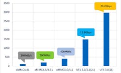
UFS 3.0 provides twice the bandwidth of UFS 2.1 and consumes less power (Fig. 2). On a single lane, UFS 3.0 is able to achieve 11.2 Gb/s, while two lanes can go up to 23.2 Gb/s. UFS 3.0 also can function at higher temperatures, which is critical for automotive applications where the temperature range is −40 to 105°C. Most embedded multimedia card (eMMC) 5.1 solutions can only handle a range of −25 to 85°C.
2. By utilizing the UFS interface, UFS 2.1 and 3.0 flash products can achieve a sequential read of approximately 2.7X and 7.1X faster than their current eMMC counterparts.
UFS 3.0 includes two features introduced specifically for the automotive market: the ability to function at an extended temperature range, supporting the wide temperature range of −40 to +105°C, and refresh operation. The data refresh feature enables greater system reliability by relocating older data to other less-used cells. What’s more, there’s temperature notification, including device alerts based on a pre-defined temperature range.
Overall, the robust structure of 3D NAND makes it a good fit in automotive applications, with the ability to withstand rugged conditions, including an automotive-grade temperature range. Also relevant to advanced automotive code-storage applications, tests have shown that data retention in a NAND device that’s subject to some 100 Program/Erase (P/E) cycles, and operating at a high temperature of 85°C, is 25 years. In an automotive application, code is highly unlikely to be subject to as many as 100 P/E cycles.
Test data also shows that the devices support more than 15 years of data retention at 70°C after 10,000 P/E cycles. That’s comparable to the performance of NOR flash products on the market today.


