It was a bit of a chore to get to this year’s Consumer Electronics Show, but it was well worth the trouble. The challenge is seeing as much as possible and then writing about it. Here are a few things I saw early on, with a lot more to come.
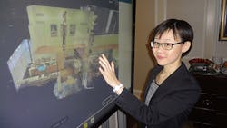
Cima NanoTech’s SANTE (self-assembling nanoparticle technology) technology supports very-large-screen capacitive touchscreens (Fig. 1). It can handle standard displays as large as 85 in., and the technology can scale to even larger displays.
blogs1. Cima NanoTechâs SANTE technology is a self assembling-nanoparticle approach that can handle this 50-in. display.
Capacitive touch is faster and easily handles multitouch supporting dozens of simultaneous contact points, compared to one or two for infrared touchscreens currently used for large displays. The nano particles wind up in a random pattern eliminating the Moire effect that is often seen on more regular touch systems.
Automotive technology is getting ever more important at CES. Marvell was highlighting 1000Baset-T1 Ethernet for the car (Fig. 2). The new standard specifies the interface, but the cabling and connectors are likely to be custom for transportation applications. The maximum run length is shorter (usually 10 to 15 meters) than regular Ethernet on CAT5 or CAT6, but the twisted pair cables are a lot smaller and lower cost. It also easily covers most cars and many larger vehicles.
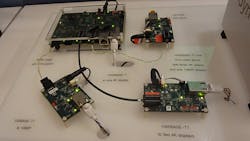
Automotive applications are the initial target for this network interface, and Marvell has a 100 Base-T1 implementation, as well. It would be ideal for other application areas like robotics, where the smaller cabling would be very useful and the more limited connection length would not be an issue.
Finally, I saw Nano Dimension’s DragonFly 2020 3D PCB printer create multilayer printed circuit boards (Fig. 3). The printer uses inkjet technology combined with a unique pair of inks, including a silver nano particle and a dielectric ink. The printer can handle boards up to around 7-by-7 in.
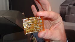
The DragonFly uses an additive approach that builds up each layer. The dielectric ink contains a collection of two tiny particles that contain the two encapsulated parts of an epoxy. The printer deposits the ink, breaks the encapsulation, and allows the epoxy to harden. This forms the circuit board, while the silver ink provides the conductive surfaces and via’s. It does not need holes because of the way the way the PCB is created.
The system is ideal for prototypes and custom solutions. There were many challenges to overcome because the characteristics of the silver ink are different from copper that would be used in conventional PCB production. Having the same characteristics is important because the prototype needs to replicate the final product. One way this is done is by increasing the vertical (Z) height when using the silver ink.
This is all I have time to write about right now, as I am off to see more of what is at CES. So stay tuned: There will be more about each of these and the other products and technologies I get to check out at CES in the near future.
About the Author
William Wong Blog
Senior Content Director
Bill's latest articles are listed on this author page, William G. Wong.
The latest blogs have been moved to alt.embedded on Electronic Design.
Bill Wong covers Digital, Embedded, Systems and Software topics at Electronic Design. He writes a number of columns, including Lab Bench and alt.embedded, plus Bill's Workbench hands-on column. Bill is a Georgia Tech alumni with a B.S in Electrical Engineering and a master's degree in computer science for Rutgers, The State University of New Jersey.
He has written a dozen books and was the first Director of PC Labs at PC Magazine. He has worked in the computer and publication industry for almost 40 years and has been with Electronic Design since 2000. He helps run the Mercer Science and Engineering Fair in Mercer County, NJ.
- Check out more articles by Bill Wong on Electronic Design
- Bill Wong on Facebook
- @AltEmbedded on Twitter
Comment About the Article
To join the conversation, and become an exclusive member of Electronic Design, create an account today!

Leaders relevant to this article: