Basic Op Amp Circuits with Quizplanation
What you'll learn:
To op amp or not
That's the P-I-D question
No coding needed.
Operational amplifiers are a basic component that are discussed in most analog electronics text books. Their origins are primarily military and Walt Jung provides a very thoroughly researched history of op amps in the classic "Chapter H" of his excellent and comprehensive 2005 book Op Amp Applications Handbook.
Back in the early days, op amps were comprised of vacuum tubes, including the venerable K2W vacuum tube op amp, which we covered extensively here on Electronic Design, which formed the basis of analog computers in the 1950s through to the early 70s. The K2W's success came from its low cost, adequate performance, and ease of use — this was primarily due to the fantastic application notes, produced by George Philbrick Researches, which illustrated the various combinations of "ops" (operations) that the K2W and its siblings could be configured to perform analog computation.
By 1969, a fledgling semiconductor industry was producing monolithic op amps in silicon, including National Semiconductor's infamous 741 op amp. It was in 1969 that National produced its app note, "AN-20," which was THE reference for semiconductor op amp circuits. It was the app note I referred to as a new grad designing telecom switching system manufacturing test gear.
Among AN-20's references, cited below, are those op amp application notes from Philbrick. The authors at National at that time included the likes of Bob Pease, who worked at Philbrick after graduating from college. AN-20 is once removed from the original op amp application notes by Philbrick and is among the first to convert those circuits to include considerations related to using monolithic, silicon devices.
The "operations" performed on voltages, fundamental to creating an analog computer, include gain/attenuation amplifiers, summation, subtraction, and mathematical integrals and differentials. With these operations, differential equations, describing/modeling system behaviors, could be interconnected to perform real-time, or even accelerated, observable system behaviors.
The same blocks could also be used in control systems for proportional, integral, and differential signal paths for closed-loop control of process setpoints. And, if you're a total geek, you can make attractor figures on your scope using a cheap analog computer, or discrete op amps.
So, rather than regurgitate, reword, and take credit for rephrasing the work of the greats, like many editors and writers have done over the years, I think it's most respectful to analog's legends that preceded us to review basic op amp configurations by simply presenting an excerpt from what I think is the best treatise on the subject — AN-20.
National was acquired by Texas Instruments, who ported AN-20, verbatim, into its own application note, SNOA621C, a full copy of which is downloadable from TI's website. The excerpt I'm presenting here, courtesy of TI, is an easy read, and includes minor corrections we made to missing information, lost in porting to SNOA621C, as well as in AN-20 itself back in 1969 (millions of eyeballs over 56 years didn't catch it to where revisions included it).
In addition, I'm including what I call a "Quizplanation" after the AN-20 excerpt. It's not really right to call these "quizzes"; we've done several including Bill Wong's programming "Quiz" series and James Morra's "Quiz" on lithium batteries. The "quiz" also provides the answers AND explanation of the answers to the question. So, Quiz + Explanation = Quizplanation.
Those who consider themselves experts can jump to the quizplanation, whereas those who are new to op amps, or need to dust off the cobwebs, should review the AN-20 excerpt. In any case, if you flub a question or two, you'll get an explanation of the most correct answer, and you can take the quiz as many times as you like.
For learning institutions (schools, colleges, universities, continuing education, maker spaces, etc.), and those who like to archive valuable references as PDFs, this blog, the quiz, and the explanations are presented as PDFs for download below. Please don't obliterate the Electronic Design logo as a thanks to us for the effort it took to create. Print as many handouts as your students need as long as our logo remains visible.
Blog PDF:
Quiz Questions PDF:
Quiz Answers PDF:
As usual, feel free to comment, point out errors, provide suggestions, and/or share battle scars in the comments section, below my bio.
So...here goes.
Enjoy,
-andyT
National Semiconductor AN-20 (TI SNOA621C) Introduction
The general utility of the operational amplifier is derived from the fact that it is intended for use in a feedback loop whose feedback properties determine the feed-forward characteristics of the amplifier and loop combination. To suit it for this usage, the ideal operational amplifier would have infinite input impedance, zero output impedance, infinite gain, and an open-loop 3-dB point at infinite frequency rolling off at 6 dB per octave. Unfortunately, the unit cost — in quantity — would also be infinite.
Intensive development of the operational amplifier, particularly in integrated form, has yielded circuits thath are quite good engineering approximations of the ideal for finite cost. Quantity prices for the best contemporary integrated amplifiers are low compared with transistor prices of five years ago [ed. note: 1964]. The low cost and high quality of these amplifiers allows for the implementation of equipment and systems functions impractical with discrete components. An example is the low frequency function generator which may use 15 to 20 operational amplifiers in generation, wave shaping, triggering, and phase-locking.
The availability of the low-cost integrated amplifier makes it mandatory that systems and equipment engineers be familiar with operational amplifier applications. This paper will present amplifier usages ranging from the simple unity-gain buffer to relatively complex generator and wave shaping circuits. The general theory of operational amplifiers is not within the scope of this paper and many excellent references are available in the literature.1,2,3,4 The approach will be shaded toward the practical, amplifier parameters will be discussed as they affect circuit performance, and application restrictions will be outlined.
The applications discussed will be arranged in order of increasing complexity in five categories: simple amplifiers, operational circuits, transducer amplifiers, wave shapers and generators, and power supplies [not in this excerpt]. The integrated amplifiers shown in the figures are, for the most part, internally compensated so frequency stabilization components are not shown; however, other amplifiers may be used to achieve greater operating speed in many circuits as will be shown in the text. Amplifier parameter definitions are contained in the Appendix [in the app note].
The Inverting Amplifier
The basic operational amplifier circuit is shown in Figure 1. This circuit gives closed-loop gain of R2/R1 when this ratio is small compared with the amplifier open-loop gain and, as the name implies, is an inverting circuit. The input impedance is equal to R1. The closed-loop bandwidth is equal to the unity-gain frequency divided by one plus the closed-loop gain.
The only cautions to be observed are that R3 should be chosen to be equal to the parallel combination of R1 and R2 to minimize the offset voltage error due to bias current and that there will be an offset voltage at the amplifier output equal to closed-loop gain times the offset voltage at the amplifier input.
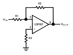
Vout = (R2/R1)*Vin
R3 = R1 || R2 for minimum error due to input bias current.
Offset voltage at the input of an operational amplifier is comprised of two components, these components are identified in specifying the amplifier as input offset voltage and input bias current. The input offset voltage is fixed for a particular amplifier, however the contribution due to input bias current is dependent on the circuit configuration used. For minimum offset voltage at the amplifier input without circuit adjustment the source resistance for both inputs should be equal. In this case the maximum offset voltage would be the algebraic sum of amplifier offset voltage and the voltage drop across the source resistance due to offset current. Amplifier offset voltage is the predominant error term for low source resistances and offset current causes the main error for high source resistances.
In high source resistance applications, offset voltage at the amplifier output may be adjusted by adjusting the value of R3 and using the variation in voltage drop across it as an input offset voltage trim.
Offset voltage at the amplifier output is not as important in AC coupled applications. Here the only consideration is that any offset voltage at the output reduces the peak to peak linear output swing of the amplifier.
The gain-frequency characteristic of the amplifier and its feedback network must be such that oscillation does not occur. To meet this condition, the phase shift through amplifier and feedback network must never exceed 180° for any frequency where the gain of the amplifier and its feedback network is greater than unity. In practical applications, the phase shift should not approach 180° since this is the situation of conditional stability. Obviously the most critical case occurs when the attenuation of the feedback network is zero.
Amplifiers which are not internally compensated may be used to achieve increased performance in circuits where feedback network attenuation is high. As an example, the LM101 may be operated at unity gain in the inverting amplifier circuit with a 15 pF compensating capacitor, since the feedback network has an attenuation of 6 dB, while it requires 30 pF in the non-inverting unity gain connection where the feedback network has zero attenuation. Since amplifier slew rate is dependent on compensation, the LM101 slew rate in the inverting unity gain connection will be twice that for the non-inverting connection and the inverting gain of ten connection will yield eleven times the slew rate of the non-inverting unity gain connection. The compensation trade-off for a particular connection is stability versus bandwidth, larger values of compensation capacitor yield greater stability and lower bandwidth and vice versa.
The preceding discussion of offset voltage, bias current and stability is applicable to most amplifier applications and will be referenced in later sections. A more complete treatment is contained in Reference 4.
>>Check out this TechXchange for similar articles and videos
The Non-Inverting Amplifier
Figure 2 shows a high input impedance non-inverting circuit. This circuit gives a closed-loop gain equal to the ratio of the sum of R1 and R2 to R1 and a closed-loop 3 dB bandwidth equal to the amplifier unity-gain frequency divided by the closed-loop gain.
The primary differences between this connection and the inverting circuit are that the output is not inverted and that the input impedance is very high and is equal to the differential input impedance multiplied by loop gain. (Open loop gain/Closed loop gain.) In DC coupled applications, input impedance is not as important as input current and its voltage drop across the source resistance.
Applications cautions are the same for this amplifier as for the inverting amplifier with one exception. The amplifier output will go into saturation if the input is allowed to float. This may be important if the amplifier must be switched from source to source. The compensation trade-off discussed for the inverting amplifier is also valid for this connection.
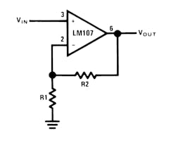
Vout = (R2+R1)/R1*Vin
R1 || R2 = Rsource for minimum error due to input bias current.
The Unity-Gain Buffer
The unity-gain buffer is shown in Figure 3. The circuit gives the highest input impedance of any operational amplifier circuit. Input impedance is equal to the differential input impedance multiplied by the open-loop gain, in parallel with common mode input impedance. The gain error of this circuit is equal to the reciprocal of the amplifier open-loop gain or to the common mode rejection, whichever is less.
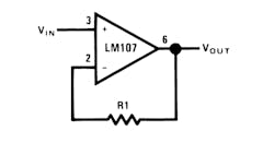
VOUT = VIN
R1 = RSOURCE for minimum error due to input bias current.
Input impedance is a misleading concept in a DC coupled unity-gain buffer. Bias current for the amplifier will be supplied by the source resistance and will cause an error at the amplifier input due to its voltage drop across the source resistance. Since this is the case, a low bias current amplifier such as the LH1026 should be chosen as a unity-gain buffer when working from high source resistances. Bias current compensation techniques are discussed in Reference 5.
The cautions to be observed in applying this circuit are three: the amplifier must be compensated for unity gain operation, the output swing of the amplifier may be limited by the amplifier common mode range, and some amplifiers exhibit a latch-up mode when the amplifier common mode range is exceeded. The LM107 may be used in this circuit with none of these problems; or, for faster operation, the LM102 may be chosen.
Summing Amplifier
The summing amplifier, a special case of the inverting amplifier, is shown in Figure 4. The circuit gives an inverted output which is equal to the weighted algebraic sum of all three inputs. The gain of any input of this circuit is equal to the ratio of the appropriate input resistor to the feedback resistor, R4. Amplifier bandwidth may be calculated as in the inverting amplifier shown in Figure 1 by assuming the input resistor to be the parallel combination of R1, R2, and R3. Application cautions are the same as for the inverting amplifier. If an uncompensated amplifier is used, compensation is calculated on the basis of this bandwidth as is discussed in the section describing the simple inverting amplifier.
The advantage of this circuit is that there is no interaction between inputs and operations such as summing and weighted averaging are implemented very easily.
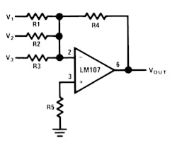
Vout = -R4 (V1/R1 + V2/R2 + V3/R3)
R5 = R1 ‖ R2 ‖ R3 ‖ R4 for minimum offset error due to input bias current
The Difference Amplifier
The difference amplifier is the complement of the summing amplifier and allows the subtraction of two voltages or, as a special case, the cancellation of a signal common to the two inputs. This circuit is shown in Figure 5 and is useful as a computational amplifier, in making a differential to single-ended conversion or in rejecting a common mode signal.
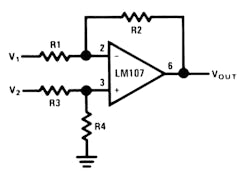
Vout = ( (R1 +R2)/(R3 + R4) ) * ( R4 / R1 ) * V2 + ( V1 * R2 / R1 )
For R1 = R3 and R2 = R4
R1 ‖ R2 = R3 ‖ R4 for minimum offset error due to input bias current
Circuit bandwidth may be calculated in the same manner as for the inverting amplifier, but input impedance is somewhat more complicated. Input impedance for the two inputs is not necessarily equal; inverting input impedance is the same as for the inverting amplifier of Figure 1 and the non-inverting input impedance is the sum of R3 and R4. Gain for either input is the ratio of R1 to R2 for the special case of a differential input single-ended output where R1 = R3 and R2 = R4. The general expression for gain is given in the figure. Compensation should be chosen on the basis of amplifier bandwidth.
Care must be exercised in applying this circuit since input impedances are not equal for minimum bias current error.
Differentiator
The differentiator is shown in Figure 6 and, as the name implies, is used to perform the mathematical operation of differentiation. The form shown is not the practical form, it is a true differentiator and is extremely susceptible to high frequency noise since AC gain increases at the rate of 6 dB per octave. In addition, the feedback network of the differentiator, R1C1, is an RC low pass filter which contributes 90° phase shift to the loop and may cause stability problems even with an amplifier which is compensated for unity gain
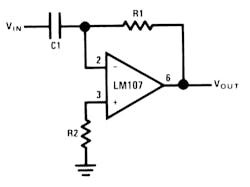
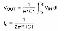
Vout = -R1C1 d/dt (Vin)
R1 = R2 for minimum offset error due to input bias current
R2 = R3 for minimum error due to input bias current.
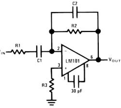
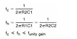
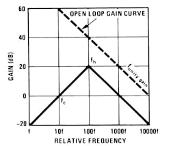
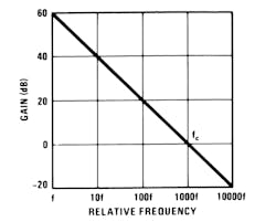
A practical differentiator is shown in Figure 7. Here both the stability and noise problems are corrected by addition of two additional components, R1 and C2. R2 and C2 form a 6 dB per octave high frequency roll off in the feedback network and R1 and C1 form a 6 dB per octave roll-off network in the input network for a total high frequency roll-off of 12 dB per octave to reduce the effect of high frequency input and amplifier noise. In addition R1C1 and R2C2 form lead networks in the feedback loop which, if placed below the amplifier unity gain frequency, provide 90° phase lead to compensate the 90° phase lag of R1C1 and prevent loop instability. A gain frequency plot is shown in Figure 8 for clarity.
R1 = R2 for minimum offset error due to input bias current
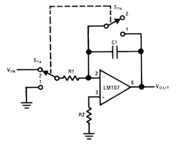
The circuit must be provided with an external method of establishing initial conditions. This is shown in the figure as S1. When S1 is in position 1, the amplifier is connected in unity gain and capacitor C1 is discharged, setting an initial condition of zero volts. When S1 is in position 2, the amplifier is connected as an integrator and its output will change in accordance with a constant times the time integral of the input voltage. The cautions to be observed with this circuit are two: the amplifier used should generally be stabilized for unity-gain operation and R2 must equal R1 for minimum error due to bias current.
Andy's Nonlinearities blog arrives the first and third Monday Tuesday of every month. To make sure you don't miss the latest edition, new articles, or breaking news coverage, please subscribe to our Electronic Design Today newsletter. Please also subscribe to Andy’s Automotive Electronics bi-weekly newsletter.
References
1. D.C. Amplifier Stabilized for Zero and Gain; Williams, Tapley, and Clark; AIEE Transactions, Vol. 67,
1948.
2. Active Network Synthesis; K. L. Su, McGraw-Hill Book Co., Inc., New York, New York.
3. Analog Computation; A. S. Jackson, McGraw-Hill Book Co., Inc., New York, New York.
4. A Palimpsest on the Electronic Analog Art; H. M. Paynter, Editor. Published by George A. Philbrick
Researches, Inc., Boston, Mass.
5. Drift Compensation Techniques for Integrated D.C. Amplifiers; R. J. Widlar, EDN, June 10, 1968.
6. A Fast Integrated Voltage Follower With Low Input Current; R. J. Widlar, Microelectronics, Vol. 1 No. 7, June 1968
>>Check out this TechXchange for similar articles and videos
About the Author

Andy Turudic
Technology Editor, Electronic Design
Andy Turudic is a Technology Editor for Electronic Design Magazine, primarily covering Analog and Mixed-Signal circuits and devices and also is Editor of ED's bi-weekly Automotive Electronics newsletter.
He holds a Bachelor's in EE from the University of Windsor (Ontario Canada) and has been involved in electronics, semiconductors, and gearhead stuff, for a bit over a half century. Andy also enjoys teaching his engineerlings at Portland Community College as a part-time professor in their EET program.
"AndyT" brings his multidisciplinary engineering experience from companies that include National Semiconductor (now Texas Instruments), Altera (Intel), Agere, Zarlink, TriQuint,(now Qorvo), SW Bell (managing a research team at Bellcore, Bell Labs and Rockwell Science Center), Bell-Northern Research, and Northern Telecom.
After hours, when he's not working on the latest invention to add to his portfolio of 16 issued US patents, or on his DARPA Challenge drone entry, he's lending advice and experience to the electric vehicle conversion community from his mountain lair in the Pacific Northwet[sic].
AndyT's engineering blog, "Nonlinearities," publishes the 1st and 3rd Tuesday of each month. Andy's OpEd may appear at other times, with fair warning given by the Vu meter pic. His cartoon series, "Inventors", appears each week in Electronic Design Weekly.
Comment About the Article
To join the conversation, and become an exclusive member of Electronic Design, create an account today!

Leaders relevant to this article: