Download this article in .PDF format
In power electronics, design engineers strive to deliver more power in a more efficient manner, and in smaller footprints at all stages of the power-delivery chain, from the smart grid to the end application. When it comes to the dc-dc link, several factors in particular are driving designs toward increased power density.
The move to portables and wearables in multiple fields is one such driver. Medical equipment that once had its own room now arrives at the patient's bedside on a cart. Desktop PCs are now tablets. And, of course, every generation of fitness band seems to cram more features into a smaller, thinner space.
In fixed-base installations, big data and the growth of the cloud has driven a massive expansion in server capacity; Amazon alone is estimated to have over 1.4 million servers, and Google uses over 260 MW of power yearly. Denser, more efficient power conversion is a key component for reducing server energy costs, and that includes cooling—one of the largest operating expenses.
At the individual device level, there's a drive toward ever-smaller devices operating at higher speeds following the curve predicted by Moore's Law, now more than 50 years old. In 1971, Intel's 4004, the first commercially available microprocessor, had a circuit density of 192 transistors/mm2, compared to 8.4 million transistors/mm2 in the current-generation Xeon Haswell-EP.Moore's Law and Power Conversion
Smaller devices operate at lower voltages and higher speeds. Although the current consumption per transistor decreases, overall consumption tends to increase since each device has so many more transistors. In response, power-supply converter designs are moving toward lower voltage, higher current, and quicker response to transient load variations. To cut resistive power losses, the trend in large-scale server and telecom applications is to employ an intermediate voltage—say, 12 or 24 V—combined with multiple point-of-load (POL) dc-dc converters.
Many systems require multiple voltages and power levels. For example, the PMP11399 is a complete PMBus power system for three ASIC/FPGA cores, DDR3 core memory, VTT termination, and auxiliary voltages commonly found on high-performance Ethernet switches. It’s a 12-V/300-W power supply with nine POL buck converters supplying six different voltages: 5, 3.3, 1.5, 1.2, 1, and 0.85 V. Power levels range from 260 mW to 60 W.
Developments in three areas are allowing designers to boost dc-dc performance while simultaneously increasing power density: more efficient control topologies; more efficient power transistors; and high-density three-dimensional packaging.
More Efficient Topologies
From the design standpoint, there are a couple of ways to get more power out of a smaller package. One is to use fewer conversion stages. To achieve this, though, the converters must offer a large ratio of input voltage to output voltage (VIN-to-VOUT). For example, a 10-to-1 ratio permits stepping down a 12-V input to as low as a 1.2-V output, while a 5-to-1 ratio only allows step-down to 2.4 V. If a device requires power at 1.2 V, then a 10-to-1 converter is needed for a single-stage solution.
Another way to reduce size is by increasing the converter’s switching frequency so that it uses smaller inductors and output capacitors. However, a tradeoff must be considered: A higher switching frequency can result in a more compact design, but it also causes extra switching losses that decrease efficiency and affect thermal performance.
The series-capacitor buck-converter topology meets these conflicting demands by blending high-frequency operation with a high VIN-to-VOUT ratio and high output current (Fig. 1). Without compromising operating efficiency, the capacitive conversion topology drastically reduces size, allowing the design of more compact applications, or the option to pack more features into the same space. The new topology also reduces the bill of materials, which can lower the overall system cost.
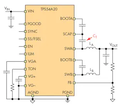
The capacitive conversion topology merges a switched-capacitor circuit with a two-phase synchronous buck converter. This design only requires one extra capacitor (the series capacitor Ct) compared to a conventional two-phase buck converter topology, but offers several advantages such as automatic current balancing between the inductors and lower switching losses.
The series capacitor Ct functions in a similar manner to the energy transfer capacitor in a SEPIC converter. As Ct alternately charges and discharges, and the FET power switches (Q2a and Q2b) open and close, the current flows alternately through the two inductors in four time intervals to establish a steady-state output at the appropriate stepped-down voltage level.
The voltage across the capacitor is nominally 50% of VIN, minimizing switching power losses, since a lower voltage swing results in less power loss per cycle. This enables higher-frequency switching with smaller inductors and capacitors, saving system space and weight.
The two-phase operation means that the on-time of both high-side switches is double that of a regular buck converter. This is particularly helpful in high-frequency, high-conversion ratio applications, because it allows for more precise control and minimizes the effect of delays due to other circuit elements.
As an example, the TPS54A20 (Fig. 2) is a two-phase, synchronous series capacitor buck converter optimized for low-voltage applications from a 12-V supply. Small, low-profile inductors significantly reduce PCB area and height. An adaptive control architecture provides fast transient response and accurate voltage regulation at up to 10-MHz operating frequency (5 MHz per phase). A phase-locked loop (PLL) locks switching signals to a reference oscillator to maintain fixed frequency operation during steady-state conditions.
New Power FETs Ease Transition to Higher Frequencies
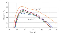
Since power MOSFETs first made their appearance, performance levels have improved in each succeeding generation by concentrating on reducing the major power losses—switching, conduction, body diode, and gate-drive losses. The TrenchFET, the most common technology, offers drastically lower switch resistance (RDS(ON)) than earlier DMOS devices. This reduces the conduction loss but at the cost of increasing the other three losses, which are due to internal capacitances. Consequently, designers must choose between a low operating frequency to optimize the efficiency or a high frequency to increase power density.
NexFET, a third-generation macrocell power MOSFET technology developed by Texas Instruments, offers an RDS(ON) comparable to TrenchFET, but reduces the parasitic capacitances by about 50% (Fig. 3). Low capacitances mean low input gate charge and short voltage transients during switching, allowing for an increase in operating frequency.
The NexFET improvement is most advantageous at 30 V and below, which is well suited for the distributed POL bus architectures popular in server and telecom applications.
3D Packaging Boosts Power Density
Increasing converter power density requires improving some key power packaging metrics. For example, reducing the parasitic capacitance and inductance is key to increasing switching frequency. And, of course, designers are always working to improve thermal efficiency.
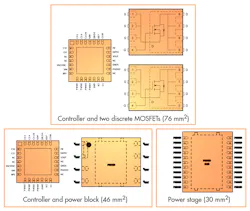
For higher power levels, each component must be optimized; a multichip module (MCM) combines a controller and power FETs into a single package for the most power-efficient overall solution. Originally, MCM designers were restricted to two dimensions, but new packages are placing components on top of each other in a three-dimensional arrangement (Fig. 4).
Three-dimensional packaging has several electrical and thermal performance benefits, as long as the individual components lend themselves to the arrangement. In a synchronous buck converter, the NexFET's vertical current flow makes it ideal for stacking. The high-side FET source terminal is then located directly above the low-side FET drain terminal, virtually eliminating resistance and parasitic inductance between the devices and enabling faster switching. In addition, the low-side source terminal is at ground potential and can be soldered directly to the exposed pad of the package for highly efficient heat transfer.
The high-current VIN (high-side FET drain) and VSW connections use clip-bonding technology, which replaces the wire-bond connection with a solid copper bridge. This substantially reduces RDS(ON) and conduction losses compared to wire bonding, and provides excellent thermal performance.
Figure 5 shows TI's PowerStack three-dimensional power package with the controller IC and NexFETs in a synchronous buck arrangement. Various configurations are available, including high-side/low-side FET combinations (power blocks) and fully synchronous buck converters.
The CSD87381P, for example, is a NexFET half-bridge power block optimized for synchronous buck applications with 5-V gate drive. This device can deliver up to 25 A with appropriate airflow and heat sinking. It is available in a 3- × 2.5-mm package, and has excellent thermal performance with a measured thermal resistance junction-to-case (θJC) of 1.65°C/W and thermal resistance junction-to-air (θJA) as low as 84°C/W.
The TPS548D22 is a 40-A synchronous buck converter in a PowerStack package suitable for storage, telecom, or similar digital high-density POL applications. The converter input-voltage range is from 1.5 up to 16 V, and VDD input-voltage range extends from 4.5 to 22 V. Output voltage ranges from 0.6 to 5.5 V.
Figure 6 shows a simplified application schematic. The switching frequency can range from 424 kHz to 1.05 MHz; for a typical application, a switching frequency of 650 kHz achieves a good balance between small solution size and high efficiency.
Conclusion
With low voltages and high currents dominating in large-scale server and telecom applications, it's critical to make the most of limited board space by increasing the power density of POL synchronous buck converters.
The optimum solution draws on multiple fields: new converter topologies, new MOSFET technology, and new packaging designs. After careful consideration of the tradeoffs, engineers can then determine the best combination of features for their applications.
About the Author
Paul Pickering
Paul Pickering has over 35 years of engineering and marketing experience, including stints in automotive electronics, precision analog, power semiconductors, flight simulation and robotics. Originally from the North-East of England, he has lived and worked in Europe, the US, and Japan. He has a B.Sc. (Hons) in Physics & Electronics from Royal Holloway College, University of London, and has done graduate work at Tulsa University. In his spare time, he plays and teaches the guitar in the Phoenix, Ariz. area
Voice Your Opinion!
To join the conversation, and become an exclusive member of Electronic Design, create an account today!

Leaders relevant to this article:


