
FPGAs have been available for more than three decades and are now a standard component in the system engineering toolbox. Embedded FPGAs (eFPGAs)—which are IP blocks for embedding FPGA fabrics into ASICs and SoCs—aren’t as familiar to many design engineers, yet they offer many similar benefits compared to standalone FPGAs, starting with hardware flexibility. Because they’re not as familiar, many myths surround the use of eFPGAs.
What follows is a closer look at several of these myths to better understand how these hardware IP blocks can be used to radically improve performance and create enormous new opportunities for end-product differentiation by adding hardware programmability to the ASIC’s or SoC’s capabilities.
1. EFPGAs are too new to work well in an ASIC or SoC design flow.
In one sense, eFPGAs are more than three decades old. There’s an eFPGA inside every packaged FPGA ever designed. Although eFPGAs as a configurable IP core for general ASIC design use are relatively new, they’re based on a well-established concept—field-programmable logic. Moreover, they’re digital IP cores, allowing for easy integration into the standard ASIC design flow.
2. EFPGAs can’t run at the same speed as other logic in the ASIC.
The real question is, “Will an eFPGA be fast enough for the application?” Often asked in another, similar way, “Is a packaged FPGA fast enough?” In the vast majority of designs, the answer is affirmative to both questions. The same design techniques that allow packaged FPGAs to deliver high performance—pipelining, parallel processing, and wide buses—also produce similar performance results with eFPGAs.
3. There’s not enough bandwidth into or out of the eFPGA for my application.
This myth may represent a problem for packaged FPGAs, which are limited by the number of I/O pins in the package. However, it’s not a problem for eFPGAs, which can have tens of thousands of I/O pins. With respect to bandwidth, a packaged FPGA is generally limited by the package—specifically the I/O pin count—and not by the underlying FPGA technology.
Embedding an eFPGA into an ASIC or SoC can result in a 10X gain in bandwidth versus a packaged FPGA. This increase in performance of the eFPGA is tied directly into the ASIC’s communications paths. I/O pin count ceases to be a concern because the eFPGA’s connectivity doesn’t rely on an IC package’s I/O pins.
In fact, I/O connectivity is one of the major reasons for embedding an eFPGA in an ASIC or SoC. Unlike packaged FPGAs, the eFPGA’s I/O pins connect directly into the IP block’s routing architecture, resulting in high-bandwidth connectivity. This connectivity may be available as parallel I/O pins or as multiple standard buses such as AXI. It’s the ASIC design team’s choice.
4. EFPGAs consume too much power.
This myth has got it backwards. The vast majority of the transistors in an eFPGA IP core either switch slowly or not at all. Those transistors dissipate virtually no power, resulting in much lower power density on the ASIC or SoC compared to other hardware IP blocks.
Many design teams using eFPGAs for the first time are quite surprised by the lower power density of an eFPGA. Using an eFPGA essentially cuts the system power consumption associated with the FPGA by half because the eFPGA eliminates the need for the packaged FPGA’s power-hungry programmable I/O. Because the eFPGA is on the ASIC die, it doesn’t need the complex programmable I/O structures that provide level translation and other sorts of I/O flexibility in packaged FPGAs.
5. Embedding eFPGAs in an ASIC or SoC adds risk.
In truth, many semiconductor foundries have already manufactured working devices that incorporate eFPGAs using multiple process technology nodes. All FPGA-based products developed and provided by Achronix on different process technologies have been fully functional. The reason for this success is simple. An eFPGA IP core is all-digital—the simplest, lowest-risk sort of IP technology to implement in a CMOS digital process technology. The result is fully functional devices.
6. Although eFPGA vendors can deliver hardware IP, their design tools aren’t fully developed.
This myth might be true for some vendors, but not for an experienced FPGA vendor such as Achronix. The company’s ACE design tool suite has been on the market for more than a decade and proven through many customer designs. ACE is the same comprehensive tool suite supplied by Achronix to support design with the company’s packaged Speedster FPGAs. This extensive, real-world use has made the ACE design tools a robust tool suite.
Tools are one of several significant differentiators among eFPGA vendors.
7. eFPGAs are hard to configure when inside an ASIC or SoC.
There’s nothing mysterious or difficult about configuring an eFPGA inside an ASIC or SoC. Every eFPGA has at least one type of configuration port and one configuration mode where a bitstream configures the eFPGA after a reset. Typically, eFPGAs have three configuration port types and configuration modes for maximum flexibility:
- JTAG
- A CPU-master mode where a CPU or other device external to the eFPGA provides the configuration bitstream.
- A flash-memory mode where the eFPGA itself downloads the configuration bitstream from an external memory or other storage device.
8. eFPGA design methodology is different than ASIC design flows.
The tools used to create designs for eFPGAs are actually quite similar to the familiar ASIC/SoC design tools. The steps in the design process are also similar: synthesis, place and route, timing analysis, and optimization. This design flow produces a bitstream used to configure the target eFPGA IP core in the system. Most vendors provide their design tools on a try-before-you-buy basis, along with any support needed to get started with design (see figure).
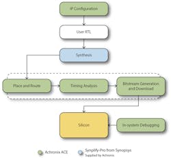
The steps in the eFPGA design process are quite similar to an ASIC design flow: synthesis, place and route, timing analysis, and optimization. (Source: Achronix)
9. The die area for an eFPGA is too big.
This myth arises from the experience working with packaged FPGAs. However, the die area associated with an eFPGA is actually significantly smaller than the die used for a packaged FPGA at the same logic density. Looking at a die of a standalone, packaged FPGA, it’s clear that the actual FPGA programmable fabric consumes roughly half of the total die area. The other half is consumed by the programmable I/O circuitry.
In the packaged FPGA domain, the programmable I/O is the real secret sauce, which is why it consumes so much die area. A packaged FPGA’s programmable I/O enables system designers to connect the FPGA to almost any other device, including microprocessors, memory, ASICs, and even other packaged FPGAs. That’s why such a huge percentage of a packaged FPGA’s die area is allocated to I/O. An eFPGA doesn’t need the programmable I/O of a packaged FPGA because it’s embedded deep inside an ASIC or SoC.
Designs implemented in packaged FPGAs typically have some percentage of the design that never changes. These "fixed functions" are required to allow the FPGA to structure data received from, or being sent to, the FPGA interfaces. For example, an FPGA with an interface to PCIe still needs to structure the data for use in the FPGA fabric. These fixed functions don’t change because they’re related to the architecture of the system, which will not change. Consequently, these fixed functions are better implemented within the ASIC or SoC because hardware programmability isn’t needed for this logic.
Not needing to implement programmable I/O and fixed functions in the eFPGA results in smaller die area than a packaged FPGA that offers the same functionality.
10. It takes too long to integrate an eFPGA IP core, delaying the ASIC/SoC design project.
This myth also arises from lack of familiarity with eFPGA IP cores. An eFPGA core drops into an ASIC or SoC just like every other digital IP core. The eFPGA has interface registers like other digital IP. Consequently, the timing closure process is the same as with other digital IP, since timing is closed between the ASIC and eFPGA interface registers. This technique is called "simple" timing mode because it follows traditional methodologies. However, it may add one stage of latency that may not be acceptable for some use cases.
There’s also an "advanced" timing mode that can be used where the timing closure is completed to the programmable registers inside the eFPGA fabric. The challenge with this mode is that the programmable nature of the eFPGA implies that the timing to the eFPGA fabric registers is design-dependent.
Achronix overcomes this challenge by including the ASIC timing in its ACE tools for any advanced timing mode path. The ASIC timing is acquired by a tool that the company created—it queries the timing of all advanced timing mode paths from the ASIC registers to the eFPGA fabric registers. This data is then added to the ACE design tools to allow for maximum performance when end users create their designs in the end product.
11. EFPGAs are too expensive.
In truth, eFPGA IP cores are no more expensive to license than other types of hardware IP cores. Moreover, using eFPGAs drives down system design costs by allowing the ASIC or SoC design team to integrate a programmable fabric correctly sized for their application. This eliminates the burden of having the unnecessary programmable I/O circuitry and the one-size-fits-all over-design of packaged FPGAs. In addition, Achronix provides the option to add custom blocks to its Speedcore eFPGA array, which can boost the effective density of the fabric, providing further cost reductions.
eFPGAs can deliver further cost savings in the following ways:
- The same SoC platform can be used to address a much wider range of applications due to the programmablity of the eFPGA. In other words, integrating an eFPGA into an SoC can create a family of products from a single die.
- Reduce SoC development risk by providing a way to implement fixes to the SoC within the eFPGA.
Moving past these myths will allow ASIC and SoC design teams to reap the many performance, flexibility, and risk-reducing benefits of eFPGAs in their designs. For more information about eFPGAs, please visit the Achronix website.
Steve Mensor is Vice President of Marketing at Achronix Semiconductor Corp.

About the Author
Steve Mensor
Vice President of Marketing
Steve has more than 25 years in senior management roles in the field-programmable-gate-array (FPGA) industry. Prior to joining Achronix, Steve was senior director of marketing at Altera (now Intel). Over his tenure at Altera, Steve managed many of the departments in marketing, including FPGA product marketing, customer and channel marketing, IP marketing and strategic partnerships, and corporate marketing. Mensor holds an MBA from Santa Clara University and a Bachelor of Science in Electrical Engineering from the University of California, Santa Barbara.
Comment About the Article
To join the conversation, and become an exclusive member of Electronic Design, create an account today!

Leaders relevant to this article: