5G Cellular Infrastructure and the Migration from FPGAs to Custom ASICs

As Zhengmao Li, executive vice president of the world’s biggest operator put it at MWC this year, 5G will require three times as many base stations to deliver the same coverage as LTE, will require three times as much power as LTE, and will cost four times as much as LTE.
Indeed, these cost/power considerations mean that the traditional 3G/4G approach to cellular infrastructure, which relied heavily on FPGAs and DSPs, is harder to justify. And cellular equipment manufacturers are turning to custom ASICs to balance tradeoffs from millimeter-wave’s (mmWave) small range; the standard’s low latency; its high throughput, its use of massive MIMO; and the need for multiple antennas, which allow mmWave to be implemented without the hand attenuating signals.
The Tradeoffs: FPGA vs. DSP vs. ASIC
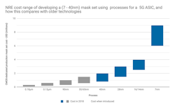
FPGAs bring flexibility and share non-recurring engineering (NRE) costs across a very large user base, they also limit development effort to the firmware required to configure them. But this comes at a cost of transistor redundancy, high power and a reduced clock performance. Indeed, the new generation of SoC FPGAs have the performance required for many of the digital components of 5G, but they don’t always address the low power and cost needs (Fig. 1), and, sometimes, will not have the required logic or on-chip memory capacity.

1. Shown are TSMC’s available processes across all functions.
Using a digital-signal-processing (DSP) approach as an alternative, for example using software from Tensilica/CEVA, is possible. But while it still gives flexibility, DSP requires significant processing capabilities and higher power in comparison to the hardwired logic of an ASIC.
The move to ASICs marks a return for the cellular infrastructure sector, but it continues a trend. ASICs for AI and autonomous vehicles have all made recent headlines in the national press, with announcements from Tesla, Facebook, Amazon, and Google. And ASICs are equally commonplace in smaller, lower-cost niche applications such as IoT, medical devices, and automotive-control systems, Using older “more than Moore” processes allows ASICs to provide a cost-effective process that balances, for example, power-consumption performance and die size, yet makes it possible to include features such as RF or MEMS sensors.
Migrating from an FPGA Design
The migration from an FPGA (such as the Xilinx Zynq) with an RF SoC will come with a significant NRE cost (Fig. 2). The use of licensable IP cores will similarly play a large part in reducing the risk and cost. To get a clearer picture of this scenario, an overview of much of the Zynq’s IP can be found in the technical reference manual for the Zynq UltraScale+.
2. ASICs optimize the number of transistors, clock cycles, production costs, and power consumption versus FPGAs/DSPs, with ASICs enabling the same performance in the soft-logic design as an FPGA that one to two nodes smaller.
The processor core, memory interfaces, and peripherals are available from Arm, Synopsys, and Cadence, respectively. High-speed serial interfaces (SerDes PHYs) and data converters can be licensed from several suppliers, including Synopsys, Cadence, or Rambus (and many others as well).
Similarly, the availability of key IPs can be licensed from third parties to replace FPGA-vendor-specific IPs. This includes a range of soft IPs such as FEC accelerators, digital downconverters (DDCs), digital upconverters (DUCs), singular-value decomposition (SVD), floating-point units (FPUs), matrix math engines, and fast-Fourier-transform (FFT) cores.
Websites like Design & Reuse are a great way of searching for this type of IP.
During the migration process of the FPGA to an ASIC, the ASIC supplier will work with its customer to make sure that good ASIC design practices are followed, such as use of clocks, resets, and coding style, and ensuring it is design-for-test (DFT) friendly. Other services are normally also provided to take the customer’s high-level system models and convert them into efficient hardware accelerators suitable for use in a SoC.
Adding Flexibility to ASICs
The key benefit of an FPGA has always been its flexibility, providing (for example) the ability to update the hardware accelerators as algorithms improve or requirements change. This has traditionally been addressed through the incorporation of high-end DSP cores, such as those from Tensilica and Ceva, or by incorporating additional high-end Arm MCUs (beyond the A53 and R5 cores that will already be part of the FPGA’s design). Adding these extra Arm MCUs also serves to simplify software development.
However, the new generation of eFPGA fabrics from Achronix, Flex Logic, and Menta gives a third route to achieving the flexibility of FPGA logic within a custom ASIC. These normally offer just a few thousand logic elements per mm2 of silicon, so using them can negate some of the power- and cost-saving benefits of an ASIC. We would recommend they be used sparingly, though, as a “get out of jail card.”
Incorporating mmWave
One of the key elements in 5G is the incorporation of mmWave frequencies, which deliver greater bandwidths. The frequency allocation varies from country to country, with the U.S.’s FCC freeing the 28-, 37-, and 29-GHz licensed bands (combined bandwidth 3.85 GHz) as well as a 14 GHz of unlicensed spectrum from 57 to 71 GHz.
For mmWave RF ASICs, from 10 to 80 GHz, CMOS processes from 55 to 22 nm will offer performance that’s suitable for many 5G applications. The smaller nodes are used to implement the not insignificant, digital logic functions needed for digital beamforming, integrated baseband processing, and embedded processor cores.
However, fully depleted silicon-on-insulator (FD-SOI) offers advantages over bulk CMOS processes for this type of application. These include improved noise figures (NF) for a given power budget, higher RF output power, better channel isolation, and the ability to scale the power and performance through adaptive body-bias techniques. And while the use of FD-SOI will increase the cost, this can be mitigated in applications like phase arrays, where the improved NF and higher power per device may mean fewer RF ICs are needed.
Conclusion—Balancing Costs in 5G
5G creates several challenges in terms of power, cost, and range, thus precipitating a shift for the cellular infrastructure sector away from FPGAs/DSPs used in 3G/4G systems and back to ASICs, which are better suited.
This doesn’t need to be the preserve of only the richest companies. Yes, the likes of Tesla, Facebook, and Google have all made headlines with multi-billion-dollar ASIC developments. But these are for AI and autonomous-driving equipment, where the most advanced technologies are essential. 5G equipment doesn’t need the same bleeding-edge technologies. As a result, costs can be lowered significantly using an ASIC approach.
For example, if we look at the demands of 5G equipment, we can assume NRE costs (including IP licensing, development, and productization) to develop a 16-nm FinFET ASIC to be in the region of about $18M, with a unit cost (based on die size, package, test time) of approximately $6.20 at volume. And NRE costs to develop a 22/28-nm ASIC would be about $14-15M, with a unit cost of approx. $9.50.
This compares with an FPGA solution, such as Xilinx’s UltraScale+ for communications applications (priced at $975 for a single unit on Digi-Key), which would have no NRE and an anticipated unit cost of about $30-50 in volume.
Assuming 1 million units per year are produced (a conservative figure), the 16-nm FinFET device is most cost effective after just 13 months (Fig. 3).
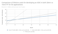
3. While having a higher NRE, a 16-nm FinFET ASIC makes it a lower-cost option after just 13 months. The graph assumes 1M units per year, NRE costs for a 28-nm ASIC at $14M, and FPGA unit cost at $40.
Obviously, as we move to cutting-edge lithography processes such as 10 nm, there would be a step change in the NRE cost for the IP licensing of PHYs, ADCs, DACs, and masking. The cost would be higher still if using 7 nm.
But, while digital 5G chips require node sizes of 7 to 40 nm, it’s worth noting the performance in the soft-logic design with an ASIC is roughly the same as for an FPGA that’s one to two nodes smaller. Putting this in context, a 22/28-nm ASIC would deliver a similar logic performance of a 16-nm FinFET FPGA, allowing costs to be brought down along with power in 5G applications.
In addition to this, the identical Arm IP used in the Xilinx UltraScale+ FPGA can be used in the ASIC, meaning the software (and the investment in software) compatible with the Xilinx device is maintained. So, despite the loss in flexibility versus an FPGA, the cost and the power provide compelling reasons why cellular equipment manufacturers are turning to custom ASICs to meet 5G’s needs.
Ian Lankshear is CEO of EnSilica.

About the Author

Ian Lankshear
CEO, EnSilica
Ian Lankshear, CEO of EnSilica, co-founded the company in 2001. Under his stewardship, the company has enjoyed sustained growth based on market-led opportunities, innovation, and export success. He has a strong technical and commercial background covering semiconductors and adjacent markets.
Ian’s early career was in radar systems development for Siemens Plessey Systems. He moved into semiconductor development in 1996, working for Hitachi and then for Nokia. Ian holds a First-Class Honors degree in Electrical & Electronics Engineering.
Comment About the Article
To join the conversation, and become an exclusive member of Electronic Design, create an account today!

Leaders relevant to this article: