Intel Buys Netspeed Systems to Stitch Together Networks Inside Chips
When Intel announced the hiring of James Keller as head of silicon engineering, the company said that his work would focus on system-on-chip (SoC) development and integration. Now the world’s largest supplier of microprocessors is trying to bolster its ability to design smaller and more efficient SoC products on shorter timelines.
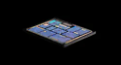
On Monday, the company said it had bought Netspeed Systems, a startup that makes software tools to automatically stitch together the network connecting all the different parts inside SoCs. That can help reduce development time and lower power and area of chip designs. These interconnects—more commonly known as the network-on-a-chip or NOC—have become more difficult to build into increasingly complex and compact chips.
“Intel is designing more products with more specialized features than ever before,” Keller, an acclaimed architect that previously worked for P.A. Semi, Apple and Advanced Micro Devices, said in a statement. “The challenge is synthesizing a broader set of IP blocks for optimal performance while reining in design time and cost,” he explained. The financial terms of the transaction were not disclosed.
Netspeed, founded by chief executive Sundari Mitra and chief technology officer Sailesh Kumar in 2011, will join Intel’s silicon engineering group. The San Jose, California-based company, which has raised $13 million in venture capital from investors including Intel Capital and Walden International, said that it would maintain existing contracts but not accept new customers. Mitra will continue to lead the team in a vice president role.
Netspeed sells software tools to many of the world’s largest chip designers, including Synopsys, Cadence, ARM and Intel. These tools are capable of connecting processor and accelerator blocks inside chips targeting automobiles, data centers, smartphones—and machine learning applications, which move massive amounts of data around SoCs. Besides enabling cache coherency, the tools make sure that the connections can support enough bandwidth to avoid becoming bottlenecks.
"Intel is dealing with the same complexity issues as everyone else,” Linley Gwennap, The Linley Group’s senior principal analyst, told Electronic Design. “They’ve designed most of their products the old fashioned way and brute-forced their way through them. And Intel can throw lots of engineers at these problems. But at some point it becomes so complicated that you have to consider using these types of automated approaches.”
The latest deal underlines another shift within the chip industry, where companies including Intel and Globalfoundries are running into the technological limits of traditional scaling. Intel has long dominated the high-stakes sector by increasing the number of transistors that can be tattooed onto silicon slabs. But as improvements have slowed in recent years, the company’s manufacturing lead has narrowed, imperiling its profitability.
Facing mounting competition in PCs and data centers, Intel has broadened its focus. The Silicon Valley company has expanded into field-programmable gate arrays (FPGAs) that can be reshaped to handle different workloads. The company, which leads the market for integrated graphics chips bundled with CPUs, has bootstrapped a new business building discrete GPUs. The team is headed by Advanced Micro Devices’ former chief architect Raja Koduri.
The company, based in Santa Clara, California, has also moved into application-specific integrated circuits for data centers and other applications. The eASIC acquisition allows customers to convert Intel’s programmable silicon into smaller, more custom chips that target specific workloads with more power efficiency by sacrificing flexibility. These chips, which are more commonly known as ASICs, can be used to run machine learning.
As traditional scaling slows, Intel is also ramping up networking and packaging investments. The company is trying to extend its new packaging technology called embedded multi-die interconnect bridge, or EMIB, into new products. The technology gives Intel the ability to combine different flecks of silicon based on different process nodes onto the same substrate, with faster interconnects bridging them together.
“Because they are struggling with Moore's Law, Intel needs to look in other directions,” Gwennap told Electronic Design. “They can’t take the same design and shrink the transistors like they used to. They are focusing more on innovations in chip design.” He added: “I wouldn't doubt that they probably looked at their own automated approaches but in this case it was probably easier to acquire the technology.”
About the Author
James Morra
Senior Editor
James Morra is the senior editor for Electronic Design, covering the semiconductor industry and new technology trends, with a focus on power electronics and power management. He also reports on the business behind electrical engineering, including the electronics supply chain. He joined Electronic Design in 2015 and is based in Chicago, Illinois.
Voice Your Opinion!
To join the conversation, and become an exclusive member of Electronic Design, create an account today!

Leaders relevant to this article:

