Leverage High-Frequency Source-Synchronous Memory in SoC Design

Download this article in PDF format.
Today’s embedded systems require high external memory bandwidth to achieve fast boot time and application loading time with minimal cost. Historically, applications such as automotive graphics, industrial systems, digital still cameras, printers, and consumer electronics have used parallel interface memories to reach that goal. Today, low-pin-count serial interfaces like the Serial Peripheral Interface (SPI) are making inroads into applications as a standard memory interface. Major systems-on-chip (SoCs) support SPI as a default configuration not only for small density memories to store configuration parameters, but also for large density memories to store application code.
However, SPI has recently increased in complexity to achieve higher bandwidth. The bus has become wider—x1/x2/x4/x8—and the data rate has expanded from single data rate (SDR) to double data rate (DDR) with frequencies above 100 MHz. The new HyperBus interface, which can also be considered as an 8-bit I/O bus DDR serial interface, has already been integrated into SoCs.
This trend improves application efficiency, such as speeding boot time and reducing application load time. at a minimal cost. However, SoC designers now face the difficulty of needing to support various serial memories. One reason is that the higher frequency requires a narrower data valid window to capture the data. Another reason is that a couple of read interfaces have been proposed by multiple memory vendors.
This article describes how SoC designers can implement a consolidated memory controller design. The focus is on the read interface (Rx domain), since the write (Tx domain) is basically identical (as a center-aligned fashion) for the serial memory interfaces discussed. Note that the protocol or Tx domain (combination of Command/Address/Data) is out of scope for this article, as it’s more likely a controller state machine design or register access control by firmware.
Data Valid Window (tDV)
When the system is running at higher frequency to achieve higher memory bandwidth, the Data Valid Window (tDV) will be narrower, especially in DDR, since data transits every half clock (SCK) cycle (Fig. 1). Because the host controller needs a certain setup-and-hold time margin to capture valid data, tDV is the main factor to limit the maximum frequency to successfully operate the memory in the system. Therefore, keeping tDV as wide as possible is crucial to consider memory timing definition.
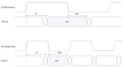
1. This comparison shows that when a system runs at a higher frequency, the Data Valid Window (tDV) will be narrower. (Source: Cypress)
There are various timing definitions in the memory industry (for example, LPDDR1, 2, 3, 4, etc.), but this article focuses on the serial memory interface of NOR flash, F-RAM, and pSRAM. These markets are shifting rapidly to the serial memory interface; in fact, various memory timing definitions are being introduced to the market.
Memory Timing Definition
Three types of DDR timing definitions will be discussed in this article. In general, SDR can be considered to have a wider timing margin if its frequency is the same as DDR. Thus, SDR will be covered when DDR timing can be met. Since the scope is the host memory controller design on the SoC, the timing definitions are categorized as Internal Clock (a), Data Learning Pattern (DLP) (b), and Strobe (RWDS/DQS) (c) based on the capturing circuit design point of view. The serial memory definition (NOR Flash, F-RAM and pSRAM) in the industry can be categorized to either of them.
Let’s look at each memory timing definition, first assuming the following host memory controller requirement:
• tDV (min) = 1.45ns
• Clock duty cycle (min) is 45% of SCK
Internal Clock
This is a legacy SPI read timing definition that outputs data per each SCK edge (DDR) (Fig. 2). The data becomes valid after tV (SCK to Output Valid) time from the SCK edge (rising edge in the example waveform), and remains valid until tHO (Output Hold) from next SCK edge (falling edge in the example waveform).
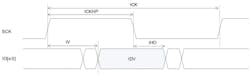
2. The DDR tDV definition of an Internal Clock: Data becomes valid after tV time (SCK to Output Valid) from the SCK edge and remains valid until tHO from the next SCK edge. (Source: Cypress)
tDV can be formulated by the following:
tDV (min) = tCKHP (min) + tHO (min) – tV (max)
where tCKHP is a half clock pulse width.
tDV must be larger than 1.45 ns as an assumption. Thus, tCKHP can be limited by the following formula. For example, Cypress’s FL-S Quad SPI memory offers tV = 6.5ns and tHO = 1.5 ns. Therefore,
tDV (min) = tCKHP (min) + tHO (min) – tV (max) > 1.45
tCKHP (min) > tV (max) – tHO (min) + 1.45 = 6.5 – 1.5 + 1.45 = 6.45 ns
When clock duty cycle is 45%, tCK (clock pulse width) will be:
tCKHP (min) = tCK * 0.45
tCK (min) = 6.45 / 0.45 = 14.3 (ns) = 69.7 (MHz)
As a result, 69.7 MHz (DDR) or 139 MHz (SDR) will be the maximum frequency used in this definition.
In the real world, the tV and tHO track each other over Process, Voltage, and Temperature (PVT). A device with a short tV has a short tHO (fast PVT) and a device with a long tV has a long tHO (slow PVT). However, this timing definition attempts to fix the tDV window offset against SCK by considering both the worst tV (tV(max)) and the worst tHO (tHO(min)) at a time shown in Figure 3, which brings fundamental frequency limitation.
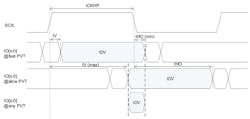
3. The DDR tDV definition of an Internal Clock across PVT. (Source: Cypress)
Since the source-synchronous memory device discussed here typically doesn’t implement delay-locked loop (DLL) nor phase-locked loop (PLL), which can compensate the timing variation across PVT in the memory device, the total uncertainness coming from PVT will be the range of 5 ns (FL-S tV varies from 1.5 ns, min, to 6.5 ns, max, across PVT). This range of uncertainness will be problematic as frequency approaches 70 MHz, where tCKHP is only 7 ns, since the host memory controller needs a certain value of tDV.
Data Learning Pattern (DLP)
The fundamental challenge as discussed above is how to track the PVT variation from a memory device at a higher SCK frequency. The new definition, called “Data Learning Pattern (DLP),” is the method that relies on the host memory controller to track PVT variation by adjusting the data sampling point to within the newly redefined tDV period (Fig. 4).

4. The DDR tDV definition of a DLP across PVT. (Source: Cypress)
The basic idea of DLP is that the tV and tHO actually track each other so that the device with a short tV has a short tHO and the device with a long tV has a long tHO. The key is that the device may guarantee the tDV width, but it may not guarantee where it exactly exists as the tDV window offset moves across PVT. It’s the host memory controller’s responsibility to track the tDV region using DLP. Now tIV is newly defined as “SCK to Output Invalid” time and tV and tIV track together across PVT. The tDV is defined by the following formula:
tDV (min) = lessor of tCKHP(min) + tIV(max) – tV(max) or tCKHP(min) + tIV(min) – tV(min)
where tCKHP is a half clock pulse width.
Identical to the earlier discussion, tDV must be greater than 1.45 ns:
tDV (min) = tCKHP (min) + tIV – tV > 1.45
tCKHP (min) > tV – tIV + 1.45
Consider “tV – tIV” as a total of cycle-to-cycle jitter and IO skew. As an assumption, 0.8 ns can be used as a realistic number. Therefore:
tCKHP (min) > 0.8 + 1.45ns = 2.25 ns
tCKHP (min) = tCK * 0.45
tCK (min) = 2.25 / 0.45 = 5 ns = 200 MHz
200 MHz (DDR) or 400 MHz (SDR) will be the maximum frequency used in this definition.
Strobe (RWDS/DQS)
Another definition for tracking the PVT validation from a memory device uses a strobe signal. The strobe, named as RWDS or DQS, is a feedback signal from the memory device that transitions at the same time with IO[x:0] across PVT, generally referred to as the “edge-aligned” strobe. The strobe and IO[x:0] are output after a certain delay from SCK, just like the “tV” definition in the previous discussion.
However, this delay is no longer used at the host-memory-controller timing definition. Instead, tDSS and tDSH against the strobe are defined as shown in Figure 5.
5. The DDR tDV definition of a Strobe across PVT. (Source: Cypress)
Now, the tDSS defines RWDS to the slowest IO valid and tDSH defines the earliest IO invalid to RWDS. The strobe (RWDS or DQS) will be a nominal 90 degrees shifted internally at the host memory controller (delayed strobe), so that the host controller captures data at the center of tDV by the delayed strobe edge.
Essentially, tDSS and tDSH define the skew between eight IOs + one RWDS = total of nine output signals from the memory device (in case eight IOs device), which can be guaranteed across PVT. Therefore, using strobe will provide more accurate timing or wider tDV window because the skew is typically in the range of much less than 1 ns. The tDV is defined by the following formula:
tDV = tCKHP (min) – tDSS (max) – tDSH (max)
where tCKHP is a half clock pulse width
Assuming tDV >1.45 ns, tDSS = tDSH = 0.4 ns, then:
tDV (min) = tCKHP (min) – tDSS (max) – tDSH (max) > 1.45
tCKHP (min) > tDSS (max) + tDSH (max) + 1.45 = 2.25 ns
tCKHP (min) = tCK * 0.45
tCK (min) = 2.25 / 0.45 = 5 ns = 200 MHz
200 MHz (DDR) or 400 MHz (SDR) will be the maximum frequency used in this definition.
Host Memory Controller Design
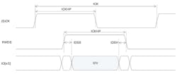
As previously discussed, timing definitions can be considered depending on the read bandwidth (frequency) target. The table compares theoretical maximum bandwidth, which can be achieved by each definition. The SoC designer can choose any one of them according to their design requirement or implement them all to support multiple serial memories, maybe with a one-time chip integration option. It would be recommended to allocate 8 bits of IOs so that single(x1)/dual(x2)/quad(x4)/octal(x8) serial memories can be supported at a time.
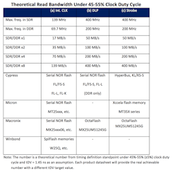
Figure 6 shows the block diagram of the capture logic that supports three required capture schemes. Each capture scheme may be implemented in a separate block and generates a capture event that triggers reading data in a register. To maximize the external memory bus frequency, the critical timing path from pad to capture register needs to be minimized, so that the capture register is placed as close to the block generating the capture event. The captured data_in may be synchronized via a FIFO into the host clock domain.
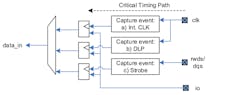
6. The block diagram shows capture logic that supports the three required capture schemes. (Source: Cypress)
Let’s break down each capture block.
Internal Clock
Figure 7 illustrates the block diagram of capture logic to support both SDR and DDR timings. The waveform shows an example of DDR timing (Fig. 8). In DDR timing, the internal clock (clk_if) can be run at twice the frequency against SCK to capture data per each rising clock. In this example, the inverted internal clock (clk_if_rx) is used to capture data. It’s recommended for host controller design to prepare an option to choose the best practice clock for capturing to cover various memories’ timings and trace delays on the PCB in this definition.

7. Here, capture logic supports both SDR and DDR timings. (Source: Cypress)

8. Shown is a timing waveform of capture logic that supports both SDR and DDR timings. (Source: Cypress)
Note: Trace delay (2xtTRACEDELAY = round trip delay) must be considered in this definition
A read transaction starts with clk_if and ends at clock input of the capturing register (clk_if_rx). Read data launches from the memory device at the rising edge of SCK and appear after tV on the external bus (I/O). Then the data propagates via IO into the host memory controller and is captured at the register in the RX clock domain with clock clk_if_rx.
Data Learning Pattern (DLP)
For higher frequencies, more accurate determination of when data needs to be captured can be achieved by using a DLP (Fig. 9). After issuing a read command, there’s a time during which the memory device prepares the requested data (sensing the data output from the memory device) as initial access latency. During this time, a known sequence of bits (DLP) is sent by the memory device to the host memory controller on every I/O pin immediately before the target data is to be output. The host can use this sequence to determine the required delays for the sampling clock (or data) in relation to data (or internal clocks) for each I/O line.

9. This block diagram represents capture logic for DLP. (Source: Cypress)
A read transaction starts with clk_if and ends at the clock input of the capturing register (clk_if_rx). Same as (a), read data launches from the memory device at the rising edge of SCK and appears after tV on the external bus (I/O). Then the data propagates via IO into the host memory controller, but the capture clock will be dynamically chosen per each read command operation depending on the comparator result. The captured data in clk_if_rx will be synchronized via a FIFO into the host clock domain (clk_if).
Data logic of delay line with comparators (Fig. 10) and DLP usage details can be found at Cypress CORE & CODE.

10. Example of logic for a delay line with comparators. (Source: Cypress)
The timing waveform of the capture logic is shown in Figure 11. In this example, the data from the memory device with fast PVT can be latched by RX_Tap_A, while the one with slow PVT can be latched by RX_Tap_D as the best practice clock.
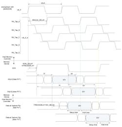
11. Shown is a timing waveform of capture logic for DLP. (Source: Cypress)
Strobe (RWDS/DQS)
The third way to capture data is to use a strobe (RWDS or DQS). This signal indicates with its rising/falling edge that the I/O lines carry valid data. For this purpose, RWDS/DQS is driven by the memory device during memory read operations. The rising/falling edge of RWDS/DQS is edge-aligned with data (Fig. 12). The host memory controller intentionally delays RWDS/DQS (Delayed RWDS/DQS = clk_if_rx(#)) a nominal 90 degrees, which is used as the capture clock at the center of tDV. tDSS defines the setup margin and the tDSH defines the hold margin. The captured data in clk_if_rx will be synchronized via a FIFO into the host clock domain (clk_if).

12. This is a block diagram of capture logic for a strobe. (Source: Cypress)
From a timing analysis standpoint, a read transaction starts with RWDS and ends at the clock input of the capturing register (clock_if_rx) (Fig. 13). There’s no critical timing relation between CK (clk_if) and RWDS (clk_if_rx); thus, the timing analysis of read transaction starts with RWDS but not from CK. It would be important for SoC designers to choose an accurate “intentional delay” as frequency becomes higher. In general, CK < 100 MHz may choose delay and CK > 100 MHz may require DLL. However, the decision must be made based on the timing analysis of each SoC design.
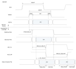
13. Timing waveform of capture logic for a strobe. (Source: Cypress)
Conclusion
There are various types of serial memories in the industry. The host memory controller in the SoC, however, can be designed as consolidated host memory controller so that the SoC is able to support multiple serial memories at one time. This strategy will mitigate the second source problem, even if the memory interface is different during each serial memory.
Daisuke Nakata is Director of Systems Engineering for the Memory Products Division at Cypress Semiconductor.

About the Author
Daisuke Nakata
Director of Systems Engineering, Memory Products Division
Daisuke Nakata is Director of Systems Engineering for the Memory Products Division at Cypress Semiconductor. He works on systems architecture development to enable the next-generation of memory products. He holds a master’s degree of materials processing from Tohoku University, Japan.
Comment About the Article
To join the conversation, and become an exclusive member of Electronic Design, create an account today!

Leaders relevant to this article: