Achieve Reliability, Availability, And Serviceability For Memory Interfaces
The world is seeing explosive growth in the aggregation of new computing, storage, and computing infrastructure equipment into data centers. These systems are being used for cloud, e-commerce, and client-server applications that connect to thin clients like tablets or smartphones. At the same time, smaller process geometries and higher operational speeds are resulting in new possibilities for errors. Users are demanding more robust techniques for preventing, repairing, and diagnosing these errors.
This file type includes high resolution graphics and schematics when applicable.
As the industry concentrates computing power and commercial value into data centers, three requirements gain importance:
• Reliability: the ability of equipment to prevent or correct errors
• Availability: the “uptime” of the equipment, the ability of the equipment to recover from errors, or the ability of the equipment to remain operational during and after an error
• Serviceability: the ease with which system administrators can diagnose problems, detect components likely to fail, and repair failing components within the equipment
Reliability, availability, and serviceability (RAS) requirements are increasing in importance to data centers. At the same time, the opportunities for errors in memory subsystems are increasing with smaller semiconductor feature sizes and higher memory transfer rates. Together, the effects of the increased importance of data integrity combined with the increasing opportunity for errors are driving the industry to develop new features within memory subsystems to improve equipment RAS.
The same features that are used to improve RAS in enterprise systems also may be used to improve RAS in applications such as automotive, military, aerospace, or medical. Strong RAS is not typically a requirement in consumer products, though, where occasional errors are tolerated, mandatory reboots are not unusual, and many consumer products cannot be repaired at all.
Related Articles
- What's The Difference Between Commodity And Embedded NAND Flash Memory?
- Key Challenges In SSD Controller Development
Most RAS features have a cost associated with them. In memory, that cost may be reduced memory bandwidth, higher memory latency, increased power, increased silicon area, or a direct cost from having to purchase additional memory to support RAS functions.
Introduction To DRAM Errors
DRAM devices store their data by storing charge on a capacitor that is formed in the DRAM device as part of the semiconductor manufacturing process. Currently, major DRAM manufacturers offer DRAM devices of over 4 billion bits (4 Gbits) on a single silicon die. Each bit cell has dimensions of a few tens of nanometers. The charge of just a few tens of femtocoulombs stored on each capacitor represents the value of each bit. As the process geometry shrinks, it becomes easier than ever to upset the value on a bit cell.
For many years, DRAM was considered perfect: shipped error-free from the manufacturer, offering the resiliency to support an infinite number of read/write cycles, no charge coupling requirements between bit cells, infallible data retention, and a zero bit error rate (BER) in transmission between the CPU and the DRAM. DRAMs are certainly very reliable and very suitable for use as-is in consumer equipment. They generally have orders of magnitude fewer errors than their flash memory cousins, but the assumption of perfect DRAM does not hold for high-reliability applications.
Sources of DRAM errors include:
• Subatomic particle strikes on the memory or on the system-on-chip (SoC) corrupting stored values: “soft errors” or “single event upsets” (SEUs)
• Physical errors in the DRAM structure that render some bits unprogrammable
• Data-dependent coupling errors where activity in one part of the DRAM corrupts a bit value in a nearby cell
• Signal integrity errors affecting the transmission of a single data bit, a group of data bits, or a command sent to the DRAM
• The complete failure of an entire DRAM device
Beginning RAS For DRAM: Parity, Hamming ECC, And BIST
There have been techniques for mitigating the effects of DRAM errors for about as long as there have been DRAM devices. Parity protection, which allows the system to detect (but not correct) DRAM errors, was used for many years. The Hamming Error Correcting Code (ECC), still in common use in systems today, was developed in 1950, over a decade before semiconductor DRAMs existed. One popular built-in self-test (BIST) algorithm for DRAM was developed in 1976. The next generation of data-center and other high-reliability systems will demand stronger RAS.
The state of the art for new high-reliability designs and the designs of the next five to 10 years will take advantage of several innovations that will improve memory interfaces’ RAS. Some of these innovations are based on existing technology, and some of them are, or soon will be, available in current or future memories. Each system will have different RAS requirements, and each memory controller and physical layer (PHY) may have different available RAS features that may increase over time.
Advanced ECC
Advanced ECC refers to a number of techniques that allow greater error correction than single-error correct, double-error detect (SECDED) based on Hamming (64,8) ECC. New high-reliability applications must solve the “dead DRAM” problem where one DRAM chip in the system may fail completely, rendering 4 or 8 bits from each data word on the DRAM interface as errors. Correcting these “dead DRAM” errors is known as S4EC-D4ED or by a number of proprietary names such as IBM’s Chipkill, Intel’s Single Device Data Correction (SDDC), HP’s Chipspare, or Sun Microsystems’ Extended ECC.
One approach to providing more advanced ECC is to extend the Hamming codes for greater correcting power. However, this generally requires more than 8 ECC check bits per 64 data bits and thus would require building custom dual-inline memory modules (DIMMs) with a greater width than the standard 72-bit (64-bit data + 8 ECC bits) width DIMM. Creating wider DIMMs and adding extra memory to support the ECC is generally costly and undesirable for most applications.
Another advanced ECC approach is to scramble the data from multiple bytes or nibbles so that each Hamming code word includes a maximum of 1 bit from any given DRAM device. In this case, the complete failure of a DRAM device is still correctable, as only 1 bit within each Hamming code word would be affected.
Advanced ECC may use block-based codes such as Reed-Solomon, Bose-Chaudhuri-Hocquenghem Coding (BCH), or low-density parity check (LDPC) that can correct for single errors or “dead DRAM” errors, but may have performance, power, or system-level implications. Possible implications of using advanced ECC using block-based codes include:
• Increased latency to implement the error detection function
• Greater increases in latency to implement the error correction function when needed
• Reduced memory bandwidth
• Increased chip area and power
• Restrictions on memory system configuration, such as the requirement to use multiple ranks of DIMM or multiple DIMMs in tandem
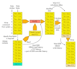
A common drawback of using ECC (parity, Hamming, or an Advanced ECC) is that when a partial or masked write operation is requested of the DDR controller, the controller must execute a read-modify-write (RMW) operation to ensure that the ECC is stored correctly (Fig. 1). This requires the underlying data to be read and merged with the bytes that are changing, and then a new parity or ECC byte is generated from the merged data. The RMW operation can take many clock cycles and can seriously impact system performance if the system tries to perform many partial write operations with parity or ECC enabled.
ECC is widely used on external memories and embedded SRAMs. Recent investigations show that single-bit upsets are no longer the dominant soft errors on today’s process nodes. Instead, multi-bit upsets are equally possible in embedded SRAMs and have a similar probability of occurrence. Therefore, traditional ECC approaches, such as Hamming code, are also considered insufficient for embedded SRAMs. New solutions for multi-bit error correction are needed to allow users to select or tune the multi-bit correction rate from traditional single-bit to double-, triple-, or quadruple-bit correction rates, depending on the application.
Not every system will choose advanced ECC. Those that do may choose to use programming to select whether advanced ECC will be used in a particular application.
Command Retry
DDR4 devices, and some DDR3 DIMMS, can assert an “alert” signal if they detect an error on the command/address bus (parity-based) or on a DDR4 write command (using a cyclic redundancy code [CRC] check). Early DDR controller implementations would simply generate an interrupt back to the system to say “something bad happened” and the system could choose to ignore it, go into reset, or take some other action. DDR controller implementations that are more advanced store a log of recent commands and can retry the failing command and the commands that were sent to the DRAM between the time of the failing command and the receipt of the alert signal.
Row Hammering Mitigation
A recently discovered source of DRAM errors is the row hammer effect, which happens when a large number of activations to a particular aggressor row in the DRAM degrades the charge on the capacitor(s) in a nearby victim row, resulting in one or more bit errors in the victim row (Fig. 2). Manufacturers have released little public information on this error, and no currently published DDR DRAM specification forbids row hammering. However, it is a significant enough issue that one manufacturer makes test equipment that can detect row hammer conditions. Emerging solutions will prevent the memory usage patterns that could cause row hammering errors, or they will use potential future memory features like targeted row refresh to prevent data loss.

Thermal Timing Parameter Adjustment
As DRAM devices increase in temperature, some characteristics like retention time may be negatively affected if the die temperature increases beyond a device-dependent threshold, increasing the probability of retention failures unless timing parameters like the refresh interval are adjusted. Newer DDR devices may contain a temperature sensor that can indicate when a temperature threshold has been crossed, typically readable from the DDR device’s mode registers. Some DDR controllers can automatically adjust temperature-related timing parameters based on this data.
On-chip Parity And On-chip ECC
Flip-flops in advanced semiconductor process geometries are susceptible to the same soft error mechanisms that cause errors in DRAM. That’s why some systems protect the memory datapath between the on-chip master and the DRAM I/O pins using parity or ECC.
Post-Package Repair
When hard errors are found after assembly or during the lifetime of the device, manufacturers may choose to repair the error rather than replace the device. This can help to repair damage to devices that are in inaccessible locations. It also may reduce the cost of manufacturing by repairing faults found during manufacturing rather than replacing them. DRAM manufacturers are working on techniques to allow users to repair DRAM devices after they have suffered damage.
In addition to identifying defective DRAMs and repairing them, designers must do the same for interconnects between the logic chip and the DRAM(s). This requires an intelligent engine to exercise at-speed test and diagnosis capabilities to pinpoint the failed interconnect or DRAM. Such an intellectual property (IP) needs to be embedded in the logic chip prior to the DDR PHY.
Conclusions
With the growing number of the possible errors of DDR DRAM devices, it is important to know which techniques can improve the RAS of enterprise, cloud, storage, or other systems that are subject to these errors. IP that incorporates RAS features can help address these issues. For example, Synopsys provides DDR Controller and PHY IP with an excellent and expanding set of RAS features as well as advanced STAR ECC IP for embedded SRAMs and STAR Memory System (SMS) for external memories’ test and diagnosis.

About the Author
Marc Greenberg
Director of Product Marketing
Marc Greenberg is the director of product marketing for DDR Controller IP at Synopsys. He has 10 years of experience working with DDR Design IP and has held technical and product marketing positions at Denali and Cadence. He has a further 10 years of experience at Motorola in IP creation, IP management, and SoC methodology roles in Europe and the United States. He holds a five-year master’s degree in electronics from the University of Edinburgh in Scotland.
Comment About the Article
To join the conversation, and become an exclusive member of Electronic Design, create an account today!

Leaders relevant to this article: