The Engineer’s Guide To High-Quality PCB Design
Virtually every electronic product is constructed with one or more printed-circuit boards (PCBs). The PCBs hold the ICs and other components and implement the interconnections between them. PCBs are created in abundance for portable electronics, computers, and entertainment equipment. They are also made for test equipment, manufacturing, and spacecraft.
Eventually, almost every EE must design a PCB, which isn’t something that’s taught in school. Yet engineers, technicians, and even novice PCB designers can create high-quality PCBs for any and every purpose with confidence that the outcome will meet or exceed the objective. Also, these designs can be completed on schedule and within budget while meeting the design requirements. Designers just need to mind the essential documentation, design steps and strategies, and final checks.


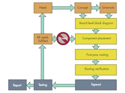
The ideal PCB design starts with the discovery that a PCB is needed and continues through the final production boards (Fig. 1). After determining why the PCB is needed, the product’s final concept should be decided. The concept includes the design’s features, the functions the PCB must have and perform, interconnection with other circuits, placement, and the approximate final dimensions.
Ambient temperature range and concerns regarding the operating environment should be addressed and used to specify the materials selected for the PCB. Components and PCB materials must be selected to guarantee operation under all expected and potential forms of duress the board may be exposed to during its lifetime.
The circuit schematic is drawn based on the concept. This detailed diagram shows the electrical implementation of each function of the PCB. With the schematic drawn, a realistic drawing of the final PCB dimensions should be completed with areas designated for each of the circuit’s schematic blocks (groups of components closely connected for electrical reasons or constraints).
Simultaneously with the schematic’s creation, the bill of materials (BOM) should be generated. The components in the circuit should be selected by analyzing the maximum operating voltages and current levels of each node of the circuit while considering tolerance criteria. With electrically satisfactory components chosen, each component should be reconsidered based on availability, budget, and size.
The BOM must be kept up-to-date with the schematic at all times. The BOM requires the quantity, reference designators, value (numeric value of ohms, farads, etc.), manufacturer part number, and PCB footprint for each component.
These five requirements are critical because they define how many of each part are needed, explain identification and circuit locations while exactly describing each circuit element used for purchasing and substitution, and explain the size of each part for area estimations. Additional descriptions may be added, but it should be a condensed list describing each circuit element, and too much information can over-complicate library development and management.
The PCB’s documents should include the hardware dimensional drawings, schematic, BOM, layout file, component placement file, assembly drawings and instructions, and Gerber file set. User guides also are useful but aren’t required. The Gerber file set is PCB jargon for the output files of the layout that are used by PCB manufacturers to create the PCB. A complete set of Gerber files includes output files generated from the board layout file:
- Silkscreen top and bottom
- Solder mask top and bottom
- All metal layers
- Paste mask top and bottom
- Component map (X-Y coordinates)
- Assembly drawing top and bottom
- Drill file
- Drill legend
- FAB outline (dimensions, special features)
- Netlist file
The special features included in the FAB outline include but are not limited to notches, cutouts, bevels, back-filled vias-in-pad (used for BGA-type IC packages that have an array of pins under the device), blind/buried vias, surface finish and leveling, hole tolerances, layer count, and more.1
Schematics control the project, so accuracy and completeness are critical for success. They include information that is necessary for the proper operation of the circuit. A schematic should include adequate design details, such as pin numbers, names, component values, and ratings (Fig. 2).
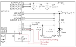
Embedded within each schematic symbol is the manufacturer part number used to determine price and specifications. The package specification determines the size of the footprint for each component. The first step should be to make sure the exposed copper for each pin is in the proper location and is slightly larger than the component pins (3 to 20 mils) depending on available area and soldering method.
Consider assembly when designing footprints, and follow the manufacturer’s recommended PCB footprint. Some components come in microscopic packages and do not allow room for extra copper. Even in these cases, a stripe of 2.5 to 3 mils of solder mask should be applied between every pin on the board.
Follow the rule of 10. Small vias have a finished hole size of 10 mils with 10 additional mils of pad ring. Traces should be 10 mils or further from the edge of the board. Trace-to-trace pitch is 10 mils (5-mil air-gap, 5-mil trace width, 1-oz copper). Vias with 40-mil diameter holes or larger should have a pad ring added for reliability. An additional 15 to 25 mils of clearance beyond the design rule should be instated for copper planes on outer layers from plane to pins. This reduces the risk of solder bridging at all solder points.
Component placement is next in the process and determined based on thermal management, function, and electrical noise considerations. A first-pass component placement step commences after the outline of component and interconnect position has been assigned. Immediately after the individual components are placed, a placement review should be held and adjustments made to facilitate routing and optimize performance.
Placement and package sizes are often reconsidered and changes are made at this point based on size and cost. Components absorbing greater than 10 mW or conducting more than 10 mA should be considered powerful enough for additional thermal and electrical considerations. Sensitive signals should be shielded from noise sources with planes and be kept impedance-controlled.
Power management components should utilize ground planes or power planes for heat flow. Make high-current connections according to the acceptable voltage drop for the connection. Layer transitions for high current paths should be made with two to four vias at each layer transition.Place multiple vias at layer transitions to increase reliability, reduce resistive and inductive losses, and improve thermal conductivity.
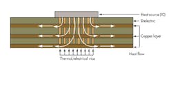
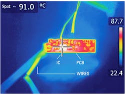
The heat generated by the IC is transferred from the device to the copper layers of the PCB (Fig. 3). The ideal thermal design will result in the entire board being the same temperature. The copper thickness, number of layers, continuity of thermal paths, and board area will have a direct impact on the operating temperature of components.
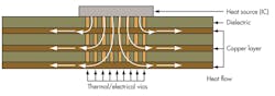
To reduce operating temperatures easily, use more layers of solid ground or power planes connected directly to heat sources with multiple vias. Establishing effective heat and high-current routes will optimize heat transfer by means of convection. The use of thermally conductive planes to spread the heat evenly dramatically lowers the temperature by maximizing the area used for heat transfer to the atmosphere (Fig. 4).2
With even heat distribution, the following formula can be used to estimate surface temperatures:
P = (heatConvection) x area x (ΔT)
where:
P = power dissipated on the board
Area = board (X axis x Y axis)
ΔT = surface temperature – ambient temperature
HeatConvection = convection constant based on ambient conditions
Fine-Tuning The Component Placement
Components should be placed in the following order: connectors, power circuits, sensitive and precision circuits, critical circuit components, and then the rest. The schematic is built around each part on the PCB and completely interconnected. Routing priority for the circuit is chosen based on power levels, noise susceptibility, or generation and routing capability.
In general, trace widths of 10 to 20 mils are used for traces carrying 10 to 20 mA and 5 to 8 mils for traces carrying less current than 10 mA. High-frequency (greater than 3 MHz) and rapidly changing signals should be carefully considered when routed along with high-impedance nodes.
The lead engineer/designer should review the layout, and physical locations and routing paths should be adjusted iteratively until the circuit is optimized for all design constraints. The number of layers depends on power levels and complexity. Add layers in pairs since the copper cladding is produced that way. The routing of power signals and planes, the grounding scheme, and the board’s ability to be used as intended all influence operation.
Final inspections should involve verification that sensitive nodes and circuits are properly shielded from noise sources, solder mask exists between pins and vias, and the silkscreen is clear and concise. When determining layer stack-up, use the first inner layer below the component sides as ground and assign power planes to other layers. Stack-ups are created in a manner that balances the board relative to the midpoint of the Z axis.
Consider any concerns the PCB designer has during the reviews, and correct the PCB based on feedback generated by the reviews. Create and verify lists of changes during each review iteration until the board is finalized. During all stages of the layout, keep the design error free by using the design rule checker (DRC).
The DRC can only catch errors that it has been programmed to monitor, and DRC rule sets often change based on individual designs. At the minimum, the design rule checking should cover package-to-package spacing, unconnected nets (a unique name identifying each node of the circuit), shorted nets, air-gap violations, if vias are too close to solder pads, if vias are too close to each other, and vertical clearance violations.
Many other important DRC rules can be set to ensure a robust design, and they should be researched and understood. For example, keep clearances at or above 5 mils. Vias should not be located within surface-mount pads (unless back-filled). And, solder mask should be between all solder points.
Cost is often a driving influence behind PCB design, so it is good to understand the cost adders in PCB manufacturing. A typical board is two to four layers, with no drill holes less than 10 mils in diameter and 5-mil minimum air gaps and trace widths. It also should be 0.062 in. thick with standard FR-4 and a copper foil weight of 1 oz. Additional layers, extra thick or thin boards, vias-in-pad, back-filled vias (non-conductive preferred due to conductivity limitations and thermal expansion differences), blind/buried vias, and lead time all substantially add to the overall cost.
Manufacturer capabilities should be understood when the PCB design commences. PCB fabs are routinely contacted about capabilities and cost reduction techniques when designing PCBs for manufacturability.
PCB design may be complex, but it is quite possible to design good boards with a little technique and practice. Using these guidelines and adding research when needed, seasoned veterans may continue honing their skills and novice designers may learn to create high-quality PCBs that exceed expectations.
1. Cohen, Patricio, Concepts and terminology used in Printed Circuit Boards (PCB), Electrosoft Engineering, Web, May 25, 2013.
2. Mauney, Charles, Thermal Considerations for Surface Mount Layouts, Texas Instruments, Web, May 13, 2013.

About the Author
Nicholaus Smith
Applications Engineer
Nicholaus Smith is an applications engineer at Integrated Device Technology with more than 10 years of experience working on printed-circuit boards (PCBs) and in semiconductor engineering. He was educated at the University of Arizona and San Jose State University while working as a technician and PCB designer. During his career, he has designed and used PCBs for engineering evaluation, customer demonstration, IC qualification, and automatic test equipment.
Comment About the Article
To join the conversation, and become an exclusive member of Electronic Design, create an account today!

Leaders relevant to this article: